

Metal gate structure and fabrication method thereof
a technology of metal gate structure and fabrication method, which is applied in the direction of semiconductor devices, electrical devices, transistors, etc., can solve the problems of reducing gate capacitance, inferior performance, and the face of conventional poly-silicon gates, and achieve the effect of reducing the thickness of the (work function) metal layer, without reducing the process throughpu
- Summary
- Abstract
- Description
- Claims
- Application Information
AI Technical Summary
Benefits of technology
Problems solved by technology
Method used
Image

Examples
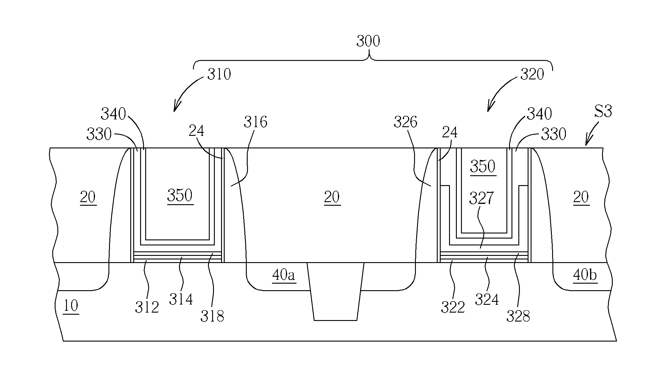
first embodiment
The First Embodiment
[0025]The substrate 10 is provided. The gate dielectric layer 110 is formed on the substrate 10. An aluminum titanium metal layer (corresponding to the metal layer 120) is formed on the gate dielectric layer 110. The titanium aluminum nitride metal layer 130 is formed in-situ on the aluminum titanium metal layer. The electrode layer 140 such as an aluminum metal layer is formed on the titanium aluminum nitride metal layer. The method of forming the titanium aluminum nitride metal layer 130 may be: importing nitrogen gas on the surface S1 of the aluminum titanium metal layer and transforming a portion of the aluminum titanium metal layer into the titanium aluminum nitride metal layer. In one embodiment, the aluminum titanium metal layer is formed by a physical vapor deposition (PVD) process. The target of the physical vapor deposition process may be one target composed of a titanium aluminum alloy; or it may be a plurality of targets respectively composed of alumi...
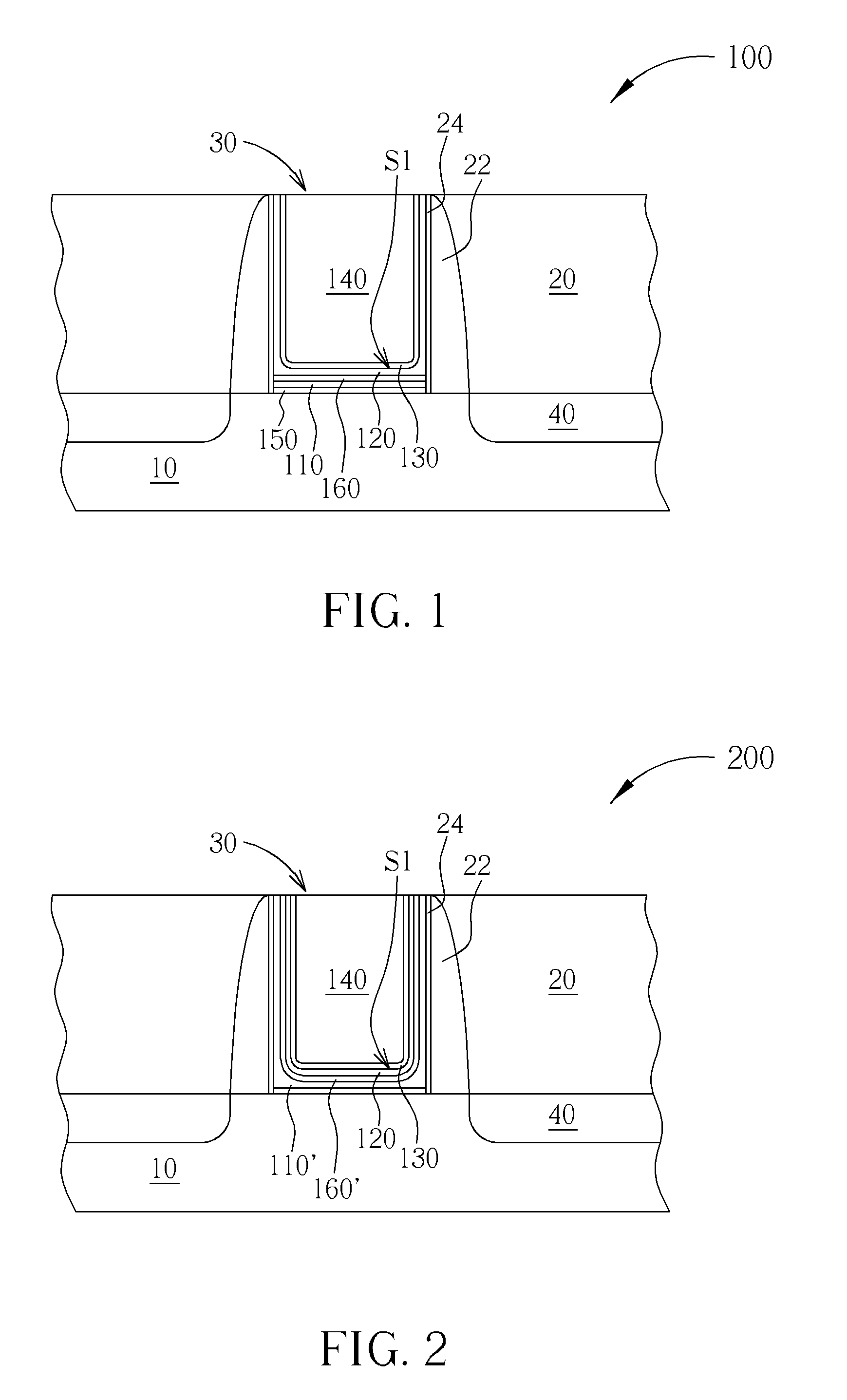
second embodiment
The Second Embodiment
[0026]The substrate 10 is provided. The gate dielectric layer 110 is formed on the substrate 10. The titanium aluminum metal layer (corresponding to the metal layer 120) is formed on the gate dielectric layer 110. A plasma nitridation process is performed to transform the surface S1 of the titanium aluminum metal layer into a titanium aluminum nitride metal layer 130. The electrode layer 140 such as an aluminum metal layer is formed on the titanium aluminum nitride metal layer 130. In one case, a plasma nitridation process may be a decoupled plasma nitridation process, but it is not limited thereto. The nitridation process, which can nitridize the surface of the titanium aluminum metal layer, can be applied to the present invention.
[0027]Furthermore, the metal gate structure 100 may further include a buffer layer 150 located between the substrate 10 and the gate dielectric layer 110 for buffering the structure difference of the substrate 10 and the gate dielectr...
PUM
| Property | Measurement | Unit |
|---|---|---|
| work function | aaaaa | aaaaa |
| size | aaaaa | aaaaa |
| penetration | aaaaa | aaaaa |
Abstract
Description
Claims
Application Information