Nitride semiconductor device and method for fabricating the same

a technology of semiconductor devices and semiconductors, applied in the field of nitride semiconductor transistors, can solve the problems of difficult to exhibit enhancement (normally off) characteristics, high sheet carrier densities at the interface, and high cost, and achieve the effect of fast switching operation and large operating curren

Active Publication Date: 2012-03-06
PANASONIC CORP
View PDF14 Cites 25 Cited by
  • Summary
  • Abstract
  • Description
  • Claims
  • Application Information

AI Technical Summary

Benefits of technology

[0011]An object of the present invention is to solve the conventional problems described above, and to provide a nitride semiconductor device which has a large operating current with normally-off operation and excellent switching characteristics.
[0014]With the nitride semiconductor device of the present invention, a forward bias voltage with respect to the channel region is applied to the control region to inject holes into the channel region. The injected holes induce generation of additional electrons in the channel region, so that the carrier concentration in the channel region is increased significantly. As a result of this, the normally-off type nitride semiconductor transistor having an increased operating current is obtained. Furthermore, the third nitride semiconductor layer is formed on the second nitride semiconductor layer, in which the distance between the surface and the channel region is enlarged and it becomes negligible to receive the influence of the surface. As a result of this, a decrease in carrier concentration in the channel region and occurrence of current collapse are prevented.
[0016]With the method for fabricating a nitride semiconductor device according to the present invention, in selectively forming the control region with p-type conductivity, the third nitride semiconductor layer does not have to be etched. Therefore, the second nitride semiconductor layer is prevented from being damaged by etching, and thereby the nitride semiconductor device of this invention shows the large operating current and fast switching operation characteristics.

Problems solved by technology

However, in the heterojunction of the nitride semiconductor, even though impurities are not added in the nitride semiconductors intentionally, spontaneous polarization and piezoelectric polarization produces high sheet carrier densities at the interface thereof.
As a result of this, most of GaN-based heterojunction FETs exhibit depletion (normally-on) characteristics, and it is difficult to exhibit enhancement (normally-off) characteristics.
However, unlike a silicon semiconductor, it is difficult to form p-type or n-type conductive areas selectively by ion implantation or thermal diffusion in the nitride semiconductors.
So it is difficult to obtain a good pn junction in this method.
This method, however, has a serious problem that the etching of the p-type nitride semiconductor layer causes electrical damages at the channel region and it is difficult to obtain good electrical properties of FETs.
Moreover, trapping of electrons into defects created on the surface of the channel region or other damage-induced influences inhibit a fast switching operation, that is, a so-called current collapse occurs.

Method used


Image

  • Nitride semiconductor device and method for fabricating the same
  • Nitride semiconductor device and method for fabricating the same
  • Nitride semiconductor device and method for fabricating the same

Examples


first embodiment

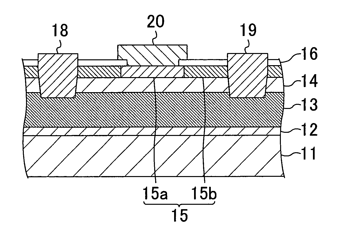
[0030]A first embodiment of the present invention will be described with reference to the accompanying drawings. FIG. 1 shows a cross-sectional structure of a nitride semiconductor transistor according to the first embodiment of the present invention.

[0031]Referring to FIG. 1, a substrate 11 is made of silicon and its principal plane is the (111) plane. A buffer layer 12 of AlN having a thickness of 100 nm is formed on the principal plane of the substrate 11.

[0032]A first nitride semiconductor layer 13 of undoped GaN having a thickness of 2 μm and a second nitride semiconductor layer 14 of undoped Al0.15Ga0.85N having a thickness of 25 nm are formed on the buffer layer 12. A channel region of the transistor which will be described later is formed in the interface region between the first nitride semiconductor layer 13 and the second nitride semiconductor layer 14.

[0033]On the second nitride semiconductor layer 14, a third nitride semiconductor layer 15 is formed which is made of Al0...

second embodiment

[0057]A second embodiment of the present invention will be described below with reference to the accompanying drawings. FIG. 5 shows a cross-sectional structure of a nitride semiconductor transistor according to the second embodiment. The description of the components shown in FIG. 5 that are the same as those shown in FIG. 1 will be omitted by retaining the same reference numerals.

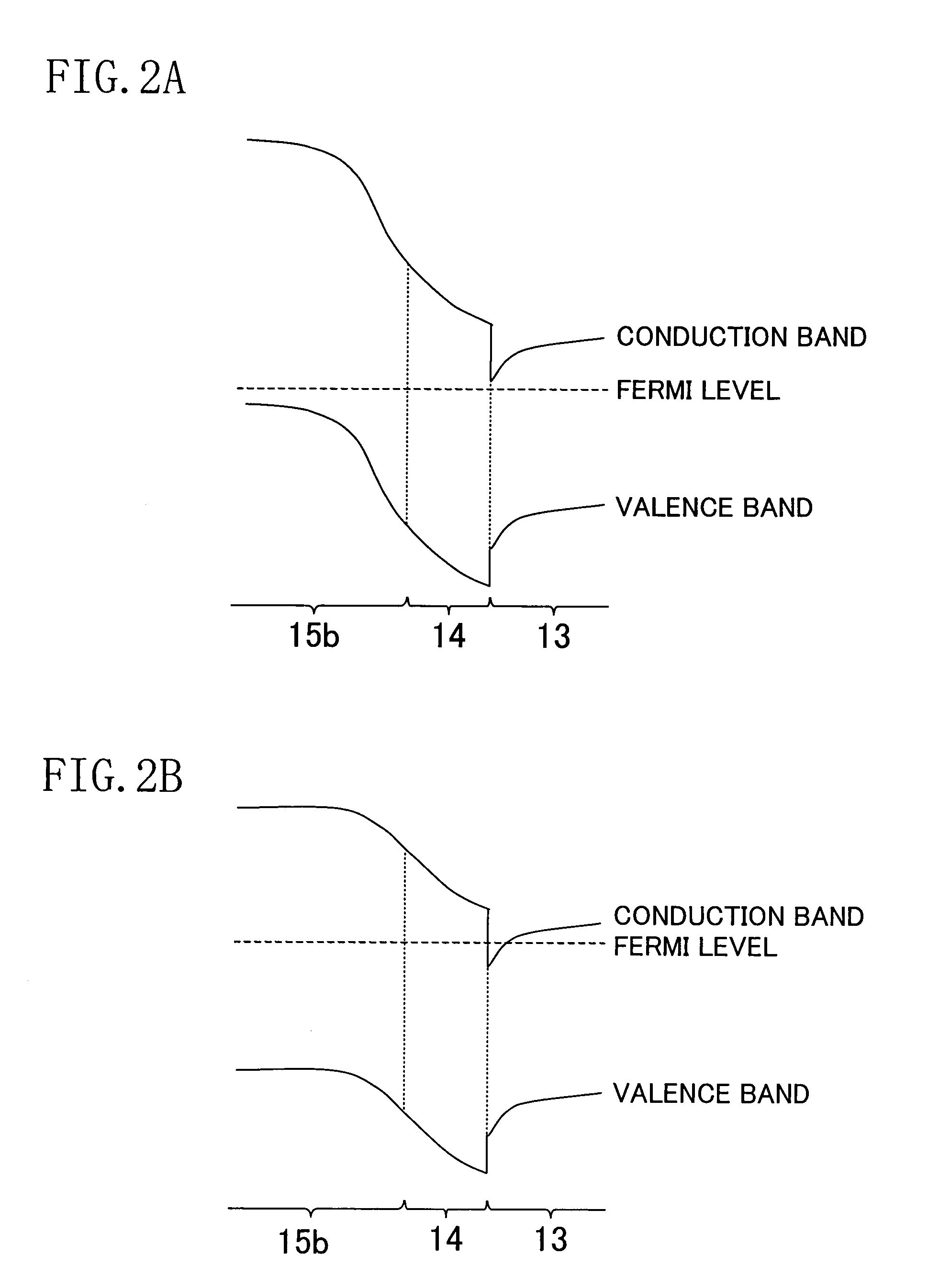
[0058]Referring to FIG. 5, the transistor according to the second embodiment has a thin portion formed in a portion of the high resistive region 15b located between the control region 15a and each of the drain electrode 19 and the source electrode 18.

[0059]As the resistance of the high resistive region 15b between the control region 15a and the drain electrode 19 is higher, a greater amount of leakage current between the gate and the drain can be reduced. The resistance of the high resistive region 15b increases with a decreasing thickness. Therefore, in the transistor of the second embodiment, the high r...

third embodiment

[0062]A third embodiment of the present invention will be described below with reference to the accompanying drawings. FIG. 7 shows a cross-sectional structure of a nitride semiconductor transistor according to the third embodiment. The description of the components shown in FIG. 7 that are the same as those shown in FIG. 5 will be omitted by retaining the same reference numerals.

[0063]Referring to FIG. 7, in the transistor according to the third embodiment, the top of the third nitride semiconductor layer 15 is formed with not a hydrogen diffusion barrier film but a hydrogen diffusion film 17 for supplying hydrogen. It is sufficient that the hydrogen diffusion film 17 is deposited by, for example, a plasma enhanced CVD method and made of silicon nitride (SiN) containing equal to or more than 1×10²⁰ / cm3 of hydrogen. The SiN film containing hydrogen releases hydrogen by a thermal treatment. Therefore, to a portion of the third nitride semiconductor layer 15 covered with the hydrogen ...


PUM


Abstract

A nitride semiconductor device includes: a first nitride semiconductor layer; a second nitride semiconductor layer formed on the first nitride semiconductor layer and having a wider band gap than the first nitride semiconductor layer; and a third nitride semiconductor layer formed on the second nitride semiconductor layer. A region of the third nitride semiconductor layer located below the gate electrode is formed with a control region having a p-type conductivity, and a region of the third nitride semiconductor layer located between the gate electrode and each of the source electrode and the drain electrode is formed with a high resistive region having a higher resistance than the that of the control region.

Description

CROSS-REFERENCE TO RELATED APPLICATIONS[0001]This application claims priority under 35 U.S.C. §119 on Patent Application No. 2006-278913 filed in Japan on Oct. 12, 2006, the entire contents of which are hereby incorporated by reference.BACKGROUND OF THE INVENTION[0002](a) Fields of the Invention[0003]The present invention relates to nitride semiconductor transistors and their fabrication methods. In particular, the present invention relates to normally-off type nitride semiconductor transistors applicable to power switching devices, and their fabrication methods.[0004](b) Description of Related Art[0005]In recent years, field effect transistors (FET) made of gallium nitride (GaN)-based materials have been widely investigated for high frequency devices and high power devices. As the GaN-based nitride semiconductor, not only GaN but also aluminum nitride (AlN), indium nitride (InN), and the like are used. Since these nitride semiconductors can form various types of compound materials,...

Claims


Application Information

Patent Timeline
Patent Type & Authority Patents(United States)
IPC IPC(8): H01L29/66
CPCH01L29/1066H01L29/4175H01L29/7783H01L29/7786H01L29/2003
Inventor UEMOTO, YASUHIROHIKITA, MASAHIROUEDA, TETSUZOTANAKA, TSUYOSHIUEDA, DAISUKE
Owner PANASONIC CORP
Why Eureka
Try Eureka