

Apparatus for inverted multi-wafer MOCVD fabrication
a technology of inverted mocvd and apparatus, which is applied in the direction of chemically reactive gases, coatings, crystal growth processes, etc., can solve the problems of preventing consistent reproduction of semiconductor devices, large and non-uniform boundary layer thickness of hot air over wafers and susceptors, and affecting device performance. , to achieve the effect of reducing the depth of the boundary layer, reducing turbulence, and easy penetration
- Summary
- Abstract
- Description
- Claims
- Application Information
AI Technical Summary
Benefits of technology
Problems solved by technology
Method used
Image

Examples
Embodiment Construction
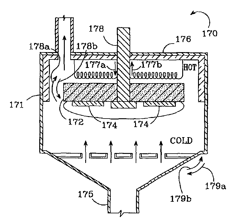
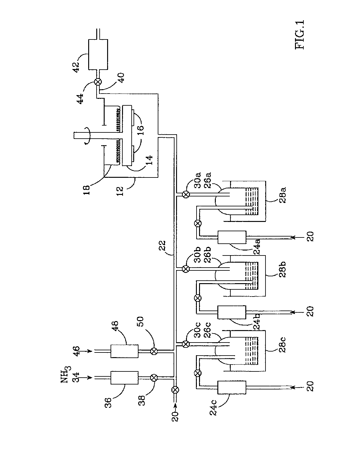
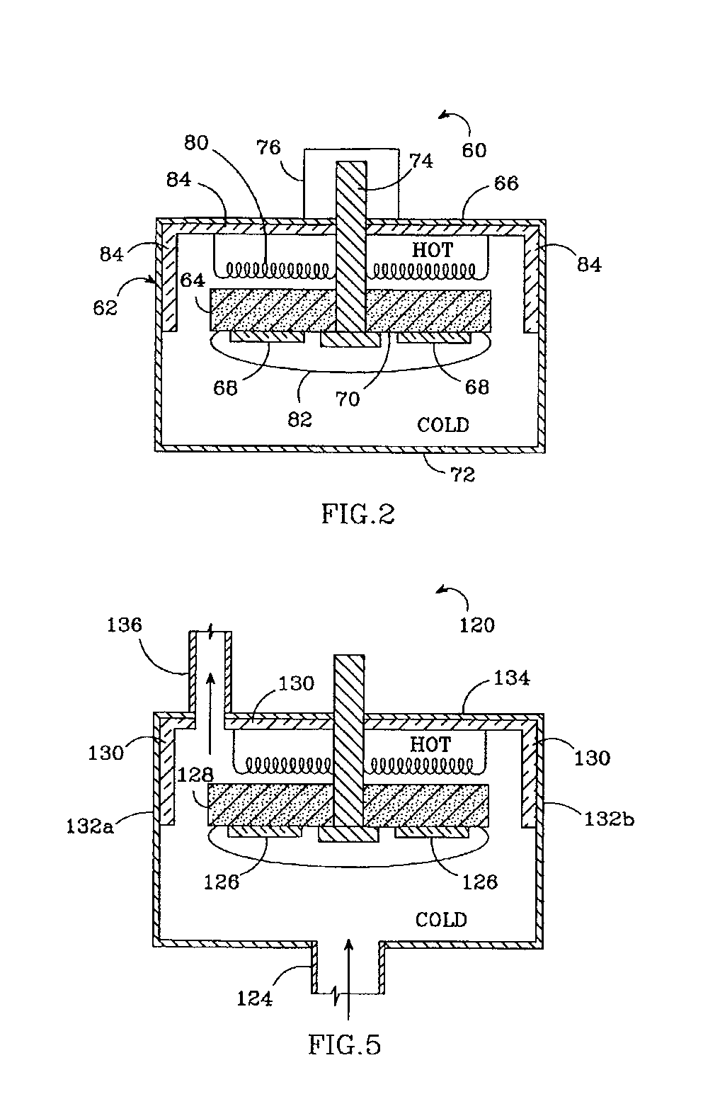
[0027]MOCVD reactors with inverted susceptors according to the present invention can be used in many different semiconductor fabrication systems, but are particularly adapted for use in MOCVD fabrication systems of the type shown in FIG. 1. MOCVD is a nonequilibrium growth technique that relies on vapor transport of precursers and subsequent reactions of Group III alkyls and Group V hydrides in a heated zone. Composition and growth rate are controlled by controlling mass flow rate and dilution of various components of the gas stream to the MOCVD reactor.
[0028]Organometallic Group III growth gas sources are either liquids such as trimethylgallium (TMGa) and trimethylaluminum (TMAl), or solids such as trimethylindium (TMIn). The organometallic sources are stored in bubblers through which a carrier gas (typically hydrogen) flows. The bubbler temperature controls the vapor pressure over source material. Carrier gas will saturate with vapor from the organometallic source and transport va...
PUM
| Property | Measurement | Unit |
|---|---|---|
| temperature | aaaaa | aaaaa |
| temperature | aaaaa | aaaaa |
| pressure | aaaaa | aaaaa |
Abstract
Description
Claims
Application Information