Coated cutting insert and manufacturing method thereof
a cutting insert and coating technology, applied in the direction of cutting inserts, superimposed coating processes, natural mineral layered products, etc., can solve the problems of difficult to identify which cutting edge portion has been used, uneven use of cutting edges in the cutting process, and impaired appearance and surface smoothness of work materials after cutting, so as to achieve easy visual recognition without affecting the appearance or surface smoothness of work materials
- Summary
- Abstract
- Description
- Claims
- Application Information
AI Technical Summary
Benefits of technology
Problems solved by technology
Method used
Image
Examples
example 1
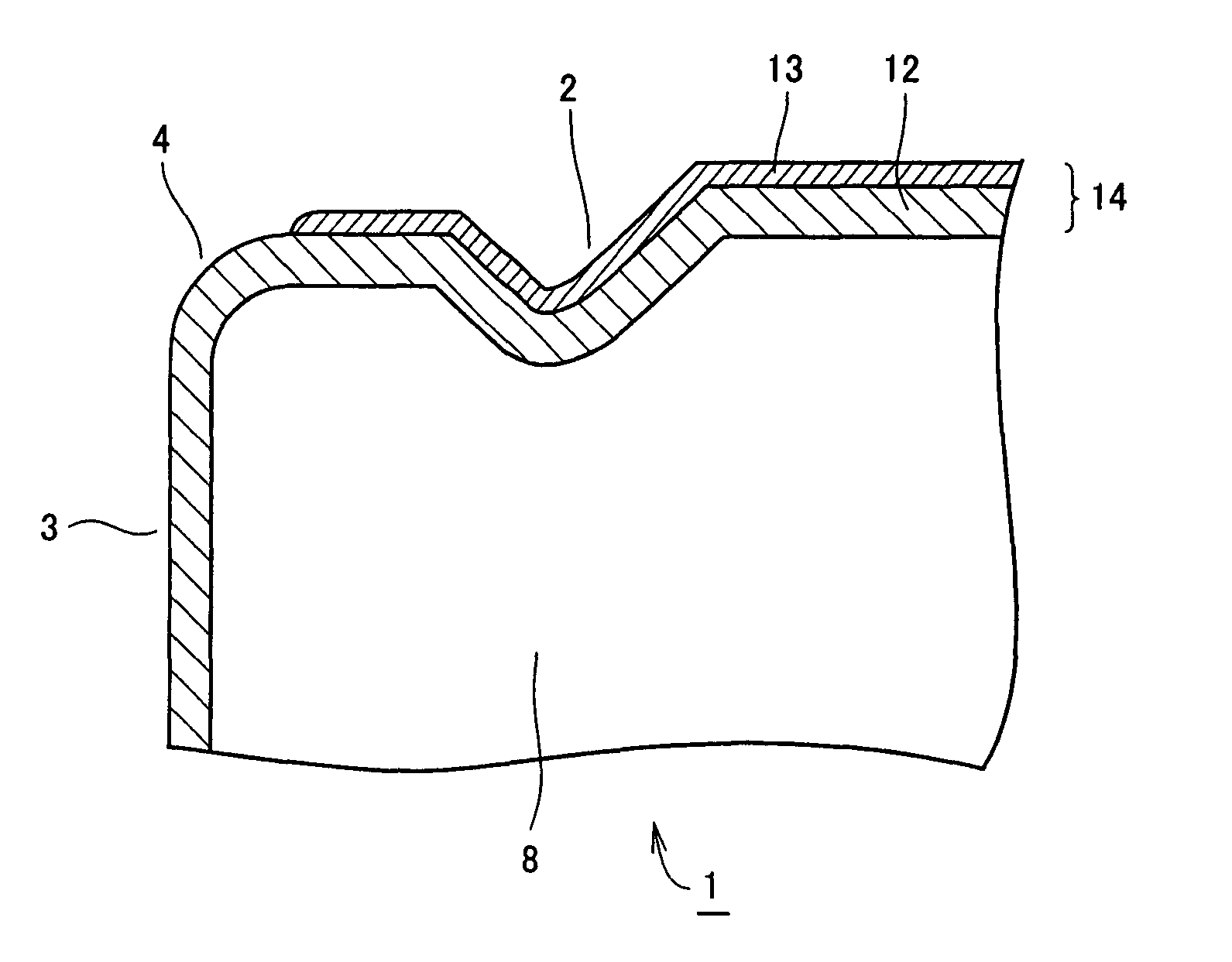
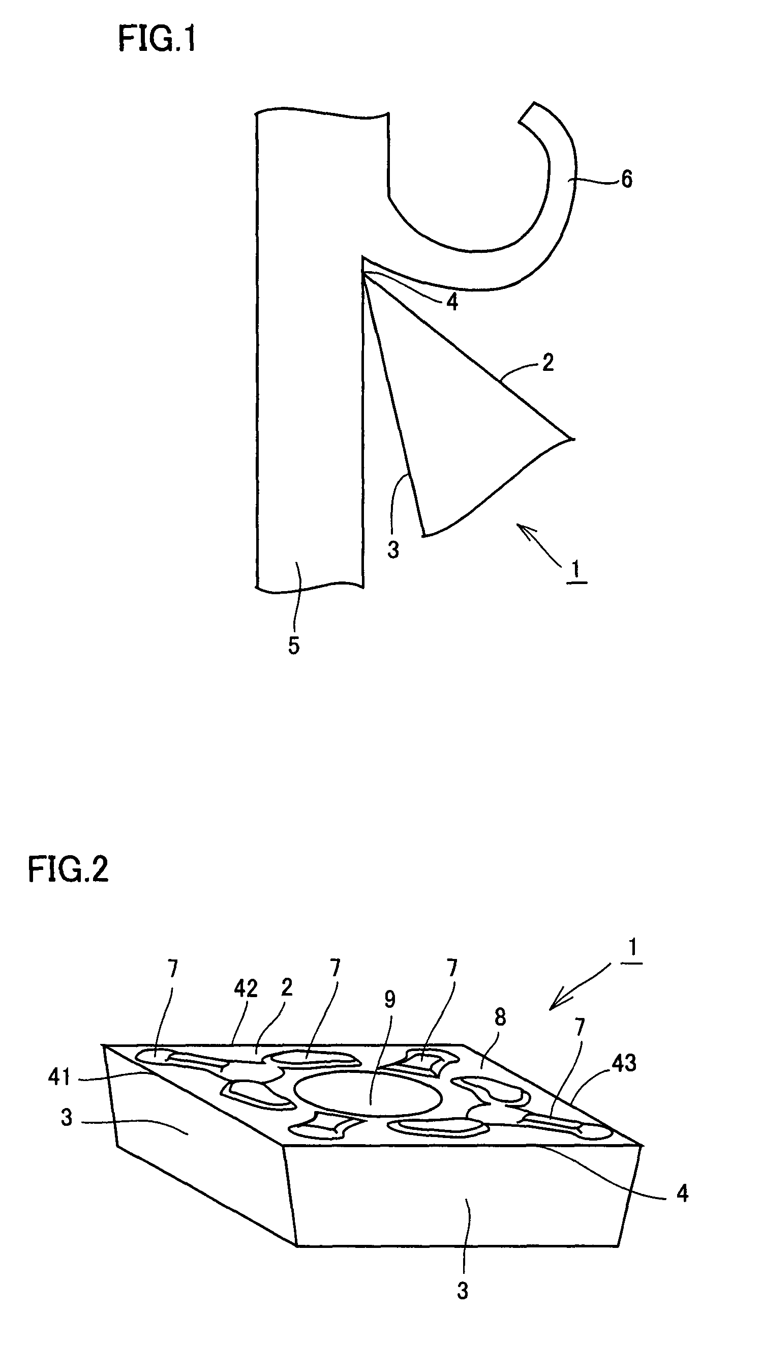
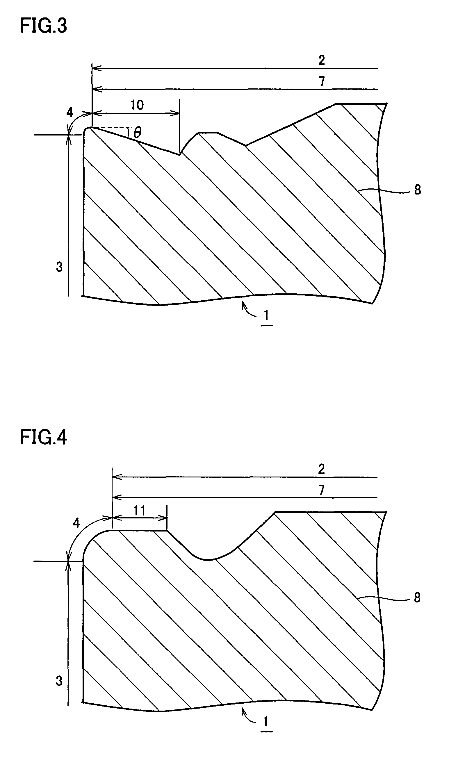
[0137]Raw material powders having a composition of 87 mass % WC, 2.5 mass % TaC, 1.0 mass % NbC, 2.0 mass % TiC and 7.5 mass % Co were pressed, and successively sintered for one hour at a temperature of 1400° C. in a vacuum atmosphere. Thereafter, the resultant sintered object was subjected to planar polishing treatment and cutting-edge treatment, thus fabricating an insert made of cemented carbide in a shape the same as that of cutting insert CNMG120408N-GU (manufactured by Sumitomo Electric Hardmetal Corp.). This insert was employed as the substrate. The substrate had 8 cutting-edge portions, 2 rake faces, and 4 flank faces. In addition, the rake face had the chip breaker formed, and adjacent to the cutting-edge portion, had the breaker recess portion inclined from the cutting-edge portion toward the central portion of the rake face to form a concave shape. The beta (β) removal layer was not formed on the surface of the substrate.
[0138]Layers listed below were successively formed ...
example 2
[0167]The substrate was obtained in a manner the same as in Example 1, except that the substrate of the coated cutting insert was shaped similarly to cutting insert SEMT13T3AGSN-L (manufactured by Sumitomo Electric Hardmetal Corp.). The substrate had 4 cutting-edge portions, 1 rake face, and 4 flank faces. In addition, the rake face had the chip breaker formed, and adjacent to the cutting-edge portion, had the breaker recess portion inclined from the cutting-edge portion toward the central portion of the rake face to form a concave shape.
[0168]Layers listed below were successively formed on the entire surface of the 1e substrate with known thermal CVD. Specifically, the substrate surface was successively coated with TiN having a thickness of 0.5 μm, TiCN (MT-CVD) having a thickness of 3.0 μm, α-alumina (Al2O3) having a thickness of 1.0 μm, and TiN having a thickness of 0.5 μm serving as the outermost layer (total thickness 5.0 μm). In this coating (referred to as coating No. 7), TiN...
example 3
[0189]The substrate employed in Example 1 was subjected to cutting-edge treatment (the cutting-edge portion was subjected to SiC brush honing treatment, and curve (R) of a radius of approximately 0.05 mm was provided to the intersection of the rake face and the flank face).
[0190]The coating the same as in Example 1 (coatings Nos. 1 to 6) coated the entire surface of the substrate.
[0191]The coated substrates were treated with the following 3 types of treatment methods C1 to C3. It is noted that, in each treatment method, the area where the indicating layer should remain was masked with a jig.
[0192](Treatment Method C1)
[0193]The coating was subjected to brushing treatment (using the diamond brush), and thereafter subjected to blasting (alumina sand #120 (average particle size 100 μm) was used and the pressure was set to 0.3 MPa), so as to remove the indicating layer on the flank face and also the indicating layer on the rake face in a region having a width of 0.18 mm from the cutting-...
PUM
| Property | Measurement | Unit |
|---|---|---|
| temperature | aaaaa | aaaaa |
| width | aaaaa | aaaaa |
| toughness | aaaaa | aaaaa |
Abstract
Description
Claims
Application Information


