Peeling apparatus and manufacturing apparatus of semiconductor device

a manufacturing apparatus and semiconductor technology, applied in the field of peeling apparatus, can solve the problems of destroying semiconductor elements, deteriorating insulations, and semiconductor elements that do not show expected characteristics, and achieve the effects of preventing electric discharge due to peeling electrification, reducing the electric resistance of the surface, and increasing the yield of the step of separating a substrate and an element formation layer from each other

Active Publication Date: 2012-03-20
SEMICON ENERGY LAB CO LTD
View PDF95 Cites 22 Cited by
  • Summary
  • Abstract
  • Description
  • Claims
  • Application Information

AI Technical Summary

Benefits of technology

[0017]It is an object of the present invention to provide an apparatus for peeling process, which is capable of preventing destruction or characteristic deterioration of a semiconductor element due to electric charge generated by peeling. In addition, in Patent Document 3, there is a limitation on the structure including the conductive film on the lower surface of the semiconductor element after peeling; however, in the present invention, it is another object to provide an apparatus for peeling process, in which a high-resistance insulating material can be selected as a material for the layer on the surface of a semiconductor element after peeling.
[0023]Electric discharge is a phenomenon in that current flows instantaneously due to high electric potential difference in a region where current is not supposed to flow, such as an insulator or a semiconductor. A surface which appears by peeling is wetted or moistened, so that electric resistivity of the surface can be decreased. Consequently, electric charge generated by peeling electrification is diffused into the wetted surface, and thus electric potential of the surface which appears by peeling is not increased so much that electric discharge is generated. By peeling with the use of an apparatus of the present invention, electric discharge due to peeling electrification can be prevented.
[0024]In a manufacturing apparatus of the present invention, electric discharge due to peeling electrification is not generated; thus, yield of a step of separating a substrate and an element formation layer from each other can be increased. In addition, characteristic deterioration of a semiconductor element due to electrostatic breakdown can be prevented; thus, a highly reliable semiconductor device can be manufactured by the present invention.
[0025]Moreover, by an apparatus of the present invention, electric charge generated by peeling is not discharged into both separated layers; thus, even if the material on the lower surface of an element formation layer is formed of an insulating material, a semiconductor element included in the element formation layer can be prevented from being destroyed due to static electricity generated by peeling electrification and characteristic deterioration of the semiconductor element can be avoided. Therefore, with respect to a peeling apparatus and a manufacturing apparatus of a semiconductor device of the present invention, a material of a peeled object is not limited and has high versatility.

Problems solved by technology

Even when the semiconductor element can operate without receiving a visible damage, a semiconductor or an insulator deteriorates due to high electric potential application and the semiconductor element does not show expected characteristics in some cases.
Therefore, when electric discharge due to static electricity is generated, the semiconductor element is destroyed, or the integrated circuit itself using the semiconductor element does not operate normally due to characteristic deterioration in some cases.
Electrostatic breakdown is one of causes which drastically reduce yield.
However, since electric discharge due to peeling electrification is generated instantaneously when two layers are separated, electricity is not removed in time by an ionizer in some cases.
However, since surfaces of two layers to be separated are charged in peeling electrification, the electric discharge does not always pass through the protective circuit.
Accordingly, in peeling electrification, electrostatic breakdown is not sufficiently prevented by the protective circuit.
Depending on an intended purpose of the stacked body, the conductive film becomes an obstacle and an expected intended purpose cannot be carried out due to the conductive film in some cases.

Method used


Image

  • Peeling apparatus and manufacturing apparatus of semiconductor device
  • Peeling apparatus and manufacturing apparatus of semiconductor device
  • Peeling apparatus and manufacturing apparatus of semiconductor device

Examples


embodiment 1

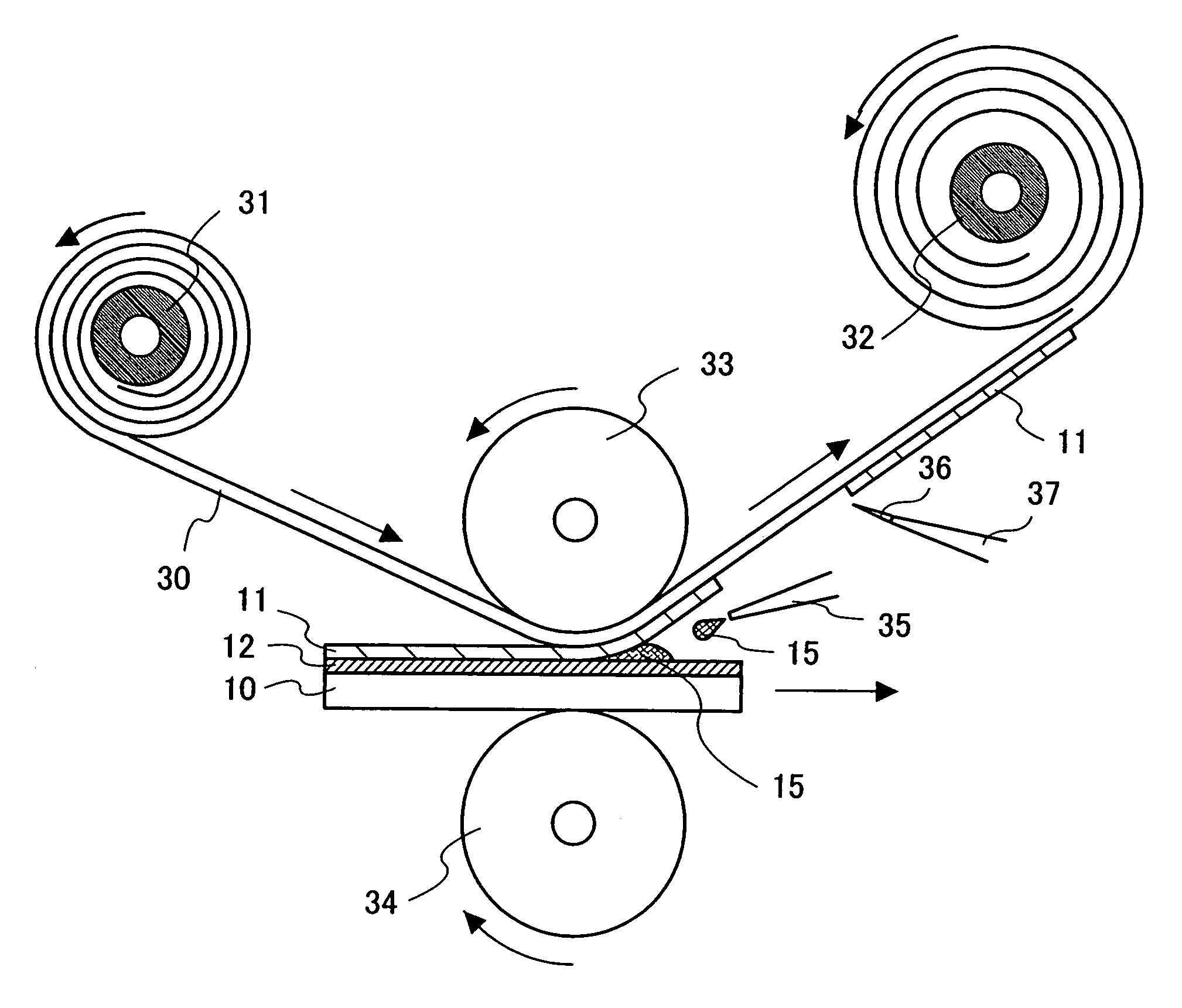
[0103]In this embodiment, a method for manufacturing a semiconductor device capable of noncontact inputting and outputting of data with the use of a peeling apparatus of the present invention will be explained. In this embodiment, an integrated circuit capable of wireless communication with 13.56 MHz signals and functioning as an IC tag is formed in an element formation layer. Hereinafter, this embodiment will be explained with reference to FIGS. 1 to 10 and FIGS. 14 to 17.

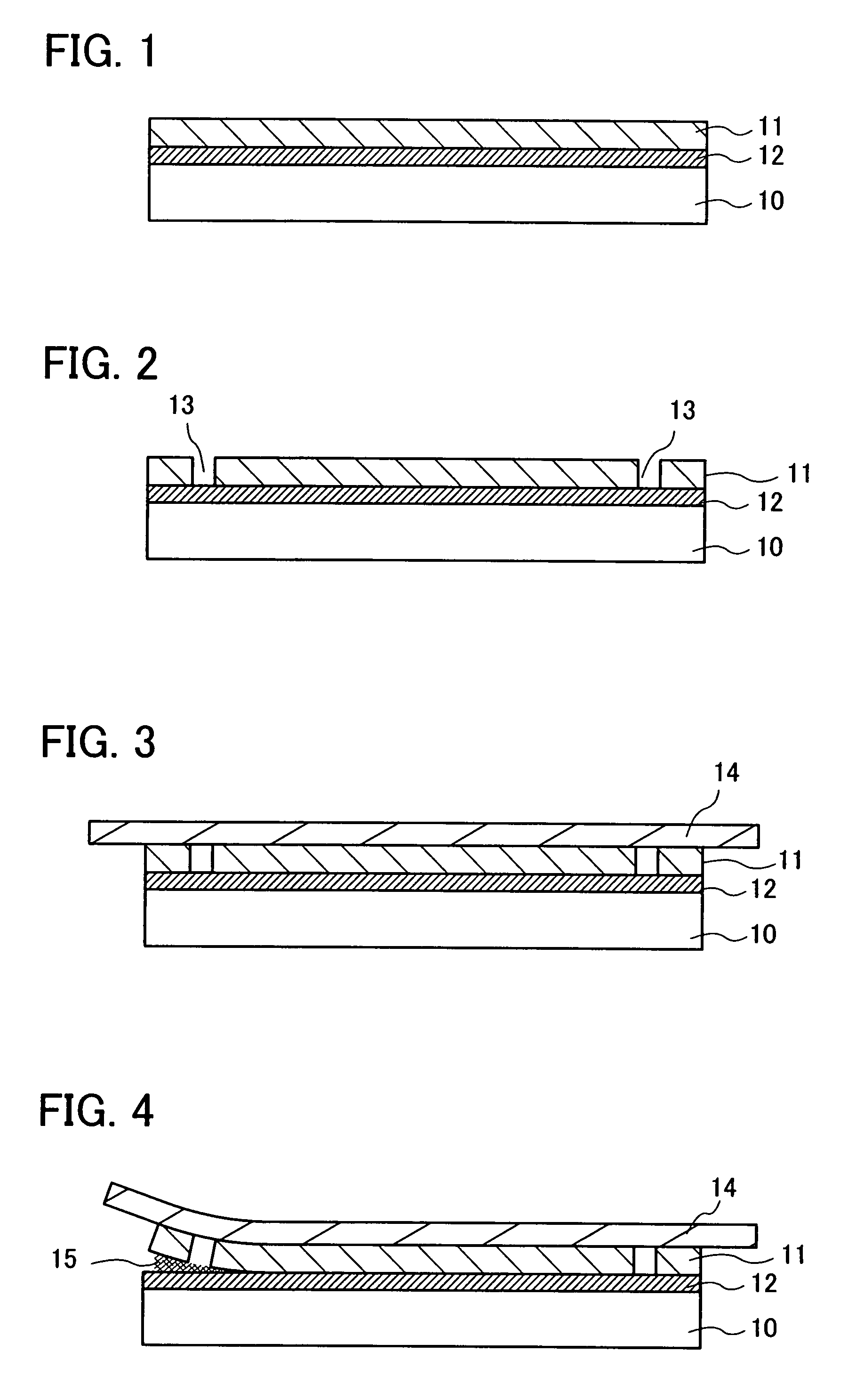
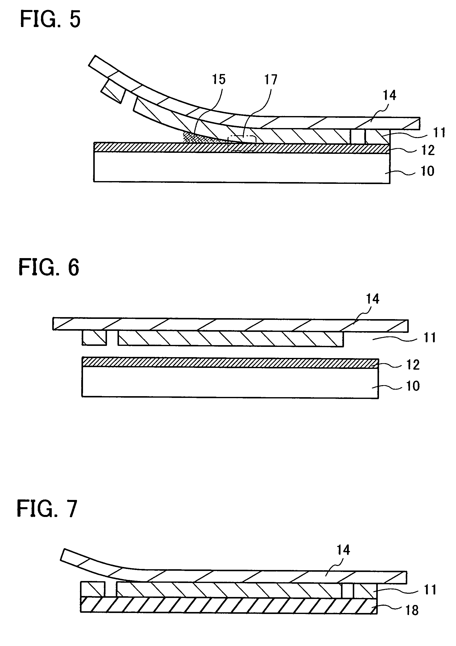
[0104]As shown in FIG. 1, a peeling layer 12 is formed over a substrate 10 and an integrated circuit is formed over the peeling layer 12. Hereinafter, a method for manufacturing the peeling layer 12 and an element formation layer 11 will be explained with reference to FIGS. 14 to 17.

[0105]As the substrate 10, a glass substrate (thickness: 0.7 mm, product name: AN100) made by Asahi Glass Co., Ltd. which is cut to have 5 inch on each side is used. As shown in FIG. 14, the peeling layer 12 had a multilayer structure ...

embodiment 2

[0124]In this embodiment, a structural example of a semiconductor device including an integrated circuit capable of wireless communication with an antenna will be explained with reference to FIGS. 18A to 18D.

[0125]FIG. 18A illustrates a structural example of an ID label as a semiconductor device of the present invention. A plurality of ID labels 161 is formed on a label board 160 (separate sheet). Each ID label 161 contains an inlet (also referred to as an inlay) 162 including an antenna and an integrated circuit which are capable of wireless communication. The ID labels 161 are put in a box 163. Information on the product and service (e.g., a product name, a brand name, a trademark, an owner of the trademark, a seller, a manufacturer, or the like) are written on the ID labels 161. On the other hand, an ID number which is peculiar to the product (or a type of the product) is stored in the integrated circuit incorporated in the inlet 162. Information which cannot be written on a surf...

embodiment 3

[0129]In this embodiment, a structural example of an active matrix liquid crystal module as a semiconductor device of the present invention will be explained with reference to FIGS. 19A and 19B. FIG. 19A is a front view of a liquid crystal module, and FIG. 19B is a cross-sectional diagram cut along a line A-A′ of FIG. 19A.

[0130]Reference numeral 200 denotes a first flexible substrate; 201 shown by a dotted line denotes a signal line driver circuit; 202 denotes a pixel portion; and 203 denotes a scanning line driver circuit. Over the first flexible substrate 200, the pixel portion 202 formed of a thin film transistor or the like, the signal line driver circuit 201, and the scanning line driver circuit 203 are formed in an element formation layer 190. The element formation layer 190 is fixed to the first flexible substrate 200 with an adhesive agent, so that a substrate for the liquid crystal module is formed. The substrate for the liquid crystal module is manufactured by any of the m...


PUM

PropertyMeasurementUnit
thicknessaaaaaaaaaa
temperatureaaaaaaaaaa
thicknessaaaaaaaaaa

Abstract

An object is to eliminate electric discharge due to static electricity generated by peeling when an element formation layer including a semiconductor element is peeled from a substrate used for manufacturing the semiconductor element. A substrate over which an element formation layer and a peeling layer are formed and a film are made to go through a gap between pressurization rollers. The film is attached to the element formation layer between the pressurization rollers. The film is bent along a curved surface of the pressurization roller on a side of the pressurization rollers, where the film is collected, and accordingly, peeling is generated between the element formation layer and the peeling layer and the element formation layer is transferred to the film. Liquid such as pure water is sequentially supplied by a nozzle to a gap between the element formation layer and the peeling layer, which is generated by peeling, so that electric charge generated on surfaces of the element formation layer and the peeling layer is diffused by the liquid.

Description

BACKGROUND OF THE INVENTION[0001]1. Field of the Invention[0002]The present invention relates to a peeling apparatus by which a layer including a structure, which is formed over a substrate, is peeled from the substrate. In particular, the present invention relates to a peeling apparatus used for manufacturing a semiconductor device, and a manufacturing apparatus of a semiconductor device for separating an element formation layer including a semiconductor element from a substrate used at the time of manufacture.[0003]In the present invention, a semiconductor device for being manufactured includes a semiconductor element that can operate by utilizing semiconductor characteristics and a general device that operates by using a plurality of semiconductor elements.[0004]As the semiconductor element, for example, a transistor, such as a MOS transistor or a thin film transistor, a diode, a MOS capacitor, and the like are given. In addition, the semiconductor device refers to an integrated ...

Claims


Application Information

Patent Timeline
Patent Type & Authority Patents(United States)
IPC IPC(8): H01L21/304
CPCB32B43/006H01L21/67132H01L21/6835H01L27/1214H01L2221/68318Y10T29/41H01L2221/68363H01L2221/68395H01L2924/19041H01L2924/30105H01L2221/6835H01L21/7813H01L27/1266H01L27/1218Y02E10/549Y02P70/50H01L31/1892H01L31/206H10K71/80H10K77/111H10K59/1201H10K2102/311H01L27/156H01L33/005H01L2221/68386G02F1/1303G02F1/13306G06K19/0772
Inventor EGUCHI, SHINGOMONMA, YOHEITANI, ATSUHIROHIROSUE, MISAKOHASHIMOTO, KENICHIHOSAKA, YASUHARU
Owner SEMICON ENERGY LAB CO LTD
Why Eureka
Try Eureka