Thermal transfer element

a technology of transfer element and lithography method, which is applied in the field of thermal transfer element, can solve the problems of reducing yield, difficult to form fine patterns, and difficulty in lithography, and achieve the effect of improving transfer characteristics and low energy consumption

Active Publication Date: 2009-03-17
SAMSUNG DISPLAY CO LTD
View PDF11 Cites 0 Cited by
  • Summary
  • Abstract
  • Description
  • Claims
  • Application Information

AI Technical Summary

Benefits of technology

[0010]The present invention solves the aforementioned problems by providing a thermal transfer element capable of improving transfer characteristics by performing the thermal transfer at low energy.
[0011]The present invention separately provides a thermal transfer element capable of facilitating delamination of a light-to-heat conversion layer and preventing the characteristics of an organic thin film layer from deteriorating.
[0013]In another exemplary embodiment according to the present invention, the thermal transfer element includes: a base substrate as a support substrate; a light-to-heat conversion layer formed on the base substrate to convert incident light to thermal energy; a transfer layer formed on the light-to-heat conversion layer to form an image; an interlayer formed between the light-to-heat conversion layer and the transfer layer to protect the light-to-heat conversion layer; and a release layer formed between the base substrate and the light-to-heat conversion layer to facilitate delamination of the light-to-heat conversion layer from the base substrate.

Problems solved by technology

The deposition method is a method of forming an organic emission layer by vacuum depositing an organic electroluminescent material using a shadow mask, but it is difficult to form a fine pattern due to deformation of the mask and difficulty in applying it to a large-sized display device.
However, the lithography method has the problem of deterioration of the characteristics of the organic emission layer due to use of a developer or an etchant of the organic electroluminescent material used to form a photoresist pattern.
The inkjet method uses a relatively simple process, but the yield is lowered and / or the thickness of the layer is irregular, and it is difficult to apply this method to a large-sized display device.

Method used


Image

  • Thermal transfer element
  • Thermal transfer element
  • Thermal transfer element

Examples


first embodiment

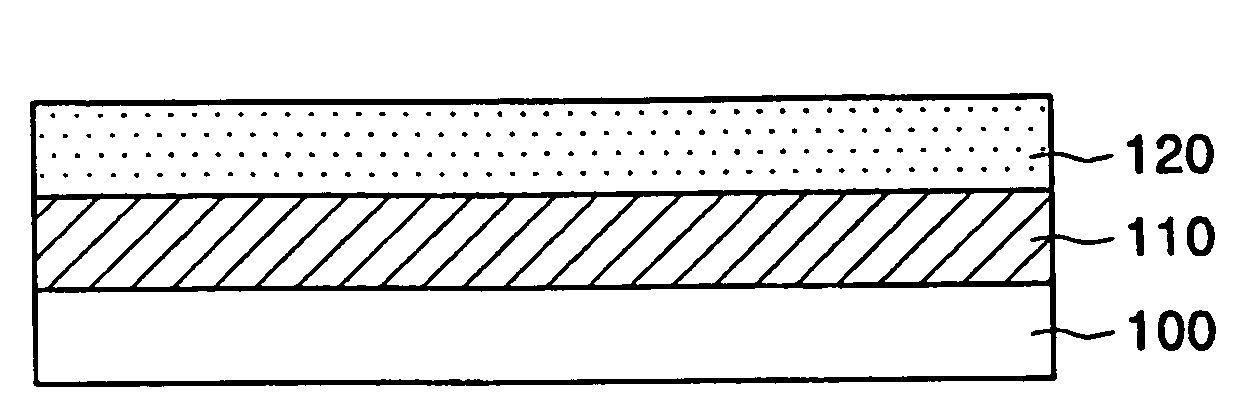
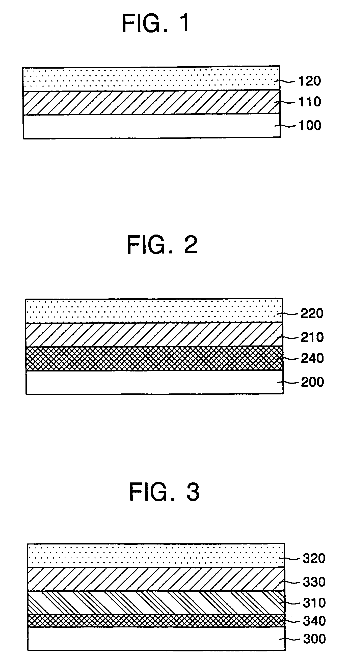
[0028]FIG. 2 is a cross-sectional view of a laser thermal transfer element for forming an organic thin film layer of an OLED in accordance with the present invention.

[0029]Referring to FIG. 2, a laser thermal transfer element in accordance with a first embodiment of the present invention includes a base substrate 200, a light-to-heat conversion (LTHC) layer 210, and a transfer layer 220. The base substrate 200 functions as a support substrate for supporting the laser thermal transfer element. The base substrate 200 is made of a transparent polymer, such as polyester, polyacryl, polyepoxy, polyethylene, polystyrene, polyethylene terephthalate or the like, and has a thickness of about 10˜500 μm. The base substrate 200 may employ a substrate, such as a glass substrate, or a film.

[0030]The LTHC layer 210 absorbs light so as to convert the light to thermal energy, and it has an appropriate optical density and includes a light-absorbing material. The light-absorbing material is a material...

second embodiment

[0038]FIG. 3 is a cross-sectional view of a laser thermal transfer element for forming an organic thin film layer of an OLED in accordance with the present invention.

[0039]Referring to FIG. 3, the thermal transfer element in accordance with a second embodiment of the present invention includes a base substrate 300, a light-to-heat conversion (LTHC) layer 310, and a transfer layer 320. The base substrate 300, the LTHC layer 310 and the transfer layer 320 are formed in a manner similar to that in the first embodiment.

[0040]The thermal transfer element in accordance with a second embodiment of the present invention further includes a release layer 340 formed between the base substrate 300 and the LTHC layer 310, and an interlayer 330 formed between the LTHC layer 310 and the transfer layer 320.

[0041]The interlayer 330, preferably, has a high thermal resistance, functions to protect the LTHC layer 310, and uses an organic layer, an inorganic layer, and a stacked layer of the organic lay...

third embodiment

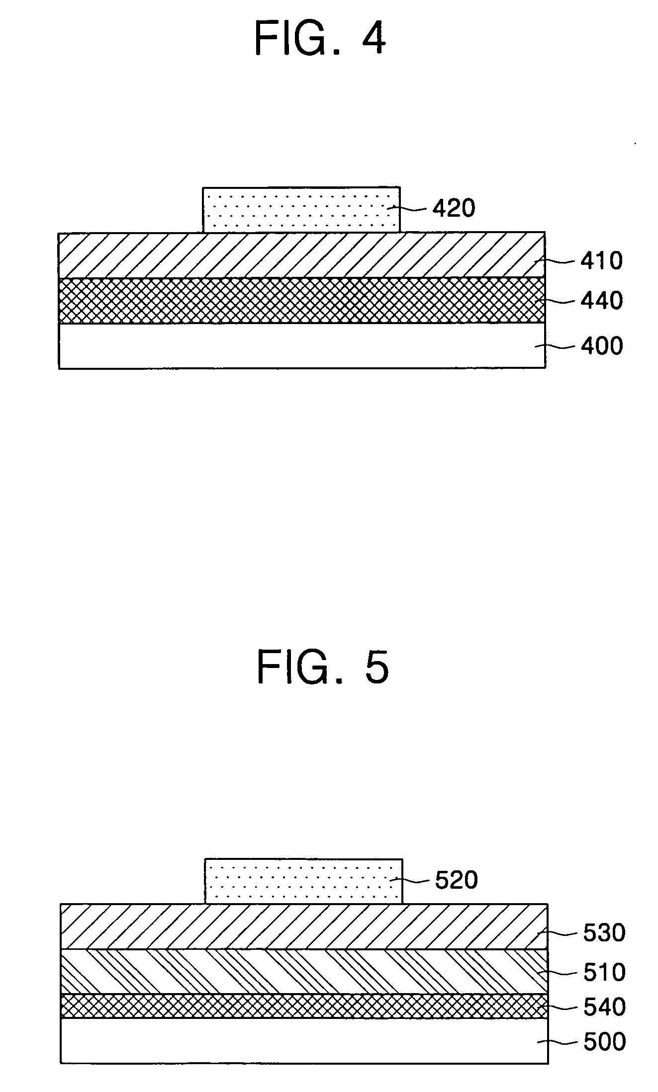
[0042]FIG. 4 is a cross-sectional view of a laser thermal transfer element for forming an organic thin film layer an OLED in accordance with the present invention.

[0043]Referring to FIG. 4, the thermal transfer element in accordance with a third embodiment of the present invention includes a base substrate 400, a light-to-heat conversion (LTHC) layer 410, and a transfer layer 420. The thermal transfer element further includes a release layer 440 formed between the base substrate 400 and the LTHC layer 410 to facilitate delamination of the LTHC layer 410 from the base substrate 400.

[0044]The base substrate 400, the LTHC layer 410 and the release layer 440 are formed in a manner similar to that in the first embodiment. Unlike the transfer layer 220 of the first embodiment, however, the transfer layer 420 is patterned. When the OLED is manufactured using the thermal transfer element in accordance with a third embodiment of the present invention, the transfer layer 420 includes at least...


PUM

PropertyMeasurementUnit
glass transition temperature Tgaaaaaaaaaa
thicknessaaaaaaaaaa
thicknessaaaaaaaaaa

Abstract

A thermal transfer element is capable of improving transfer characteristics because transfer is performed at a low temperature. The thermal transfer element includes: a base substrate as a support substrate; a light-to-heat conversion layer formed on the base substrate to convert incident light to thermal energy; a transfer layer formed on the light-to-heat conversion layer to form an image; and a release layer formed between the base substrate and the light-to-heat conversion layer to facilitate delamination of the light-to-heat conversion layer from the base substrate. The release layer includes a silicon polymer having a glass transition temperature (Tg) of 25° C. or less, and low surface energy. In a further embodiment, the thermal transfer element includes an interlayer formed between the light-to-heat conversion layer and the transfer layer to protect the light-to-heat conversion layer.

Description

CLAIM OF PRIORITY[0001]This application makes reference to, incorporates the same herein, and claims all benefits accruing under 35 U.S.C. §119 from an application for earlier filed in the Korean Intellectual Property Office on 24 Feb. 2004 and there duly assigned Serial No. 2004-12397.BACKGROUND OF THE INVENTION[0002]1. Field of the Invention[0003]The present invention relates to a thermal transfer element and, more particularly, to a thermal transfer element capable of improving transfer characteristics by performing thermal transfer at a low temperature.[0004]2. Description of the Related Art[0005]In general, an organic electroluminescent display device (OLED) includes an anode electrode formed on an insulating substrate as a lower electrode, an organic thin film layer formed on the anode electrode, and a cathode electrode formed on the organic thin film layer as an upper electrode. The organic thin film layer includes at least one of a hole injection layer, a hole transport laye...

Claims


Application Information

Patent Timeline
Patent Type & Authority Patents(United States)
IPC IPC(8): B41M5/46H05B33/10B32B27/00B41M5/40B41M5/42B41M5/44G12B15/06H01L51/00H01L51/40H01L51/50H05B33/02H05B33/12H05B33/14H05K7/20
CPCB41M5/42B41M5/443B41M2205/06B41M2205/12B41M2205/38H01L51/0013H10K71/18A01G9/021G09F23/00G09F2023/0025
Inventor KIM, MU-HYUNCHIN, BYUNG-DOOSUH, MIN-CHULYANG, NAM-CHOULLEE, SEONG-TAEK
Owner SAMSUNG DISPLAY CO LTD
Why Eureka
Try Eureka