
Circuit providing load isolation and noise reduction

a load isolation and circuit technology, applied in the field of circuits, can solve the problems of increasing memory access time, changing wave characteristics, and impairing the performance of the system, and achieve the effect of reducing noise in one or more signals

Inactive Publication Date: 2012-04-10
NETLIST INC
View PDF84 Cites 88 Cited by
  • Summary
  • Abstract
  • Description
  • Claims
  • Application Information

AI Technical Summary

Benefits of technology

[0008]Certain embodiments described herein include a memory module comprising a printed circuit board comprising at least one connector configured to be operatively coupled to a memory controller of a computer system. The memory module comprises a plurality of memory devices on the printed circuit board and a circuit. The circuit comprises a first set of ports comprising a plurality of bi-directional ports, each port of the first set of ports operatively coupled to at least one memory device of the plurality of memory devices. The memory module further comprises a second set of ports comprising one or more bi-directional ports, each port of the second set of ports operatively coupled to the at least one connector. The memory module of certain embodiments comprises a switching circuit configured to selectively operatively couple one or more ports of the second set of ports to one or more ports of the first set of ports. The one or more ports of the first set of ports and the one or more ports of the second set of ports each comprise a correction circuit in certain embodiments. The correction circuit reduces noise in one or more signals transmitted between the one or more ports of the first set of ports and the one or more ports of the second set of ports.
[0009]A method of using a memory module with a computer system is described in certain embodiments. The method includes providing a memory module comprising a printed circuit board having at least one connector configured to be operatively coupled to a memory controller of a computer system and to a plurality of memory devices. The memory module further including a circuit which comprises a first set of ports comprising a plurality of bi-directional ports, each port of the first set of ports operatively coupled to at least one memory device of the plurality of memory devices. The circuit further comprises a second set of ports comprising one or more bi-directional ports. Each port of the second set of ports is operatively coupled to the at least one connector. The circuit is configured to selectively operatively couple one or more ports of the second set of ports to one or more ports of the first set of ports in some embodiments. The one or more ports of the first set of ports and the one or more ports of the second set of ports each comprise a correction circuit. The correction circuit reduces noise in one or more signals transmitted between the one or more ports of the first set of ports and the one or more ports of the second set of ports. The method includes activating the circuit to selectively operatively couple at least one of the one or more ports of the second set of ports to at least one of the one or more ports of the first set of ports. The method also includes activating the circuit to reduce noise in the one or more signals.
[0010]Certain embodiments are described herein provide a circuit comprising a first set of ports comprising a plurality of bi-directional ports. Each port of the first set of ports may be configured to be operatively coupled to at least one memory device of a plurality of memory devices on a printed circuit board. The circuit further comprises a second set of ports comprising one or more bi-directional ports, each port of the second set of ports configured to be operatively coupled to at least one connector on the printed circuit board. The at least one connector is configured to be operatively coupled to a memory controller of a computer system. The circuit further comprises a switching sub-circuit configured to selectively operatively couple one or more ports of the second set of ports to one or more ports of the first set of ports. The one or more ports of the first set of ports and the one or more ports of the second set of ports each comprise a correction circuit in certain embodiments. The correction circuit can reduce noise in one or more signals transmitted between the one or more ports of the first set of ports and the one or more ports of the second set of ports.
[0011]In certain embodiments, a circuit comprises a first set of ports comprising a plurality of bi-directional ports. Each port of the first set of ports can be configured to be operatively coupled to at least one subsystem of a plurality of subsystems. The circuit may comprise a second set of ports comprising one or more bi-directional ports, each port of the second set of ports configured to be operatively coupled to at least one subsystem of one or more subsystems. In certain embodiments, the circuit comprises a switching sub-circuit configured to selectively operatively couple one or more ports of the second set of ports to one or more ports of the first set of ports. The one or more ports of the first set of ports and the one or more ports of the second set of ports each comprise a correction circuit in certain embodiments. The correction circuit can reduces noise in one or more signals transmitted between the one or more ports of the first set of ports and the one or more ports of the second set of ports.

Problems solved by technology

However, higher speed processors and higher memory densities translate to higher power dissipation and increased memory access time, impairing the performance of the system.
In such systems, signal reflections may occur, changing wave characteristics and degrading system performance.
These signal reflections may cause signal distortions and signal integrity issues which can contribute to reduced system performance and eventual failure of the system, thereby limiting the effectiveness of the multiplexer and / or demultiplexer in addressing the signal integrity and power dissipation issues.
Generating controllable address and device select signals can introduce timing delays on the device select, address, and control paths.
In addition, this arrangement does not address the power dissipation and may degrade performance degradation by, for example, requiring that secondary control signals be generated for the memory devices.

Method used


Image

  • Circuit providing load isolation and noise reduction
  • Circuit providing load isolation and noise reduction
  • Circuit providing load isolation and noise reduction

Examples


Embodiment Construction

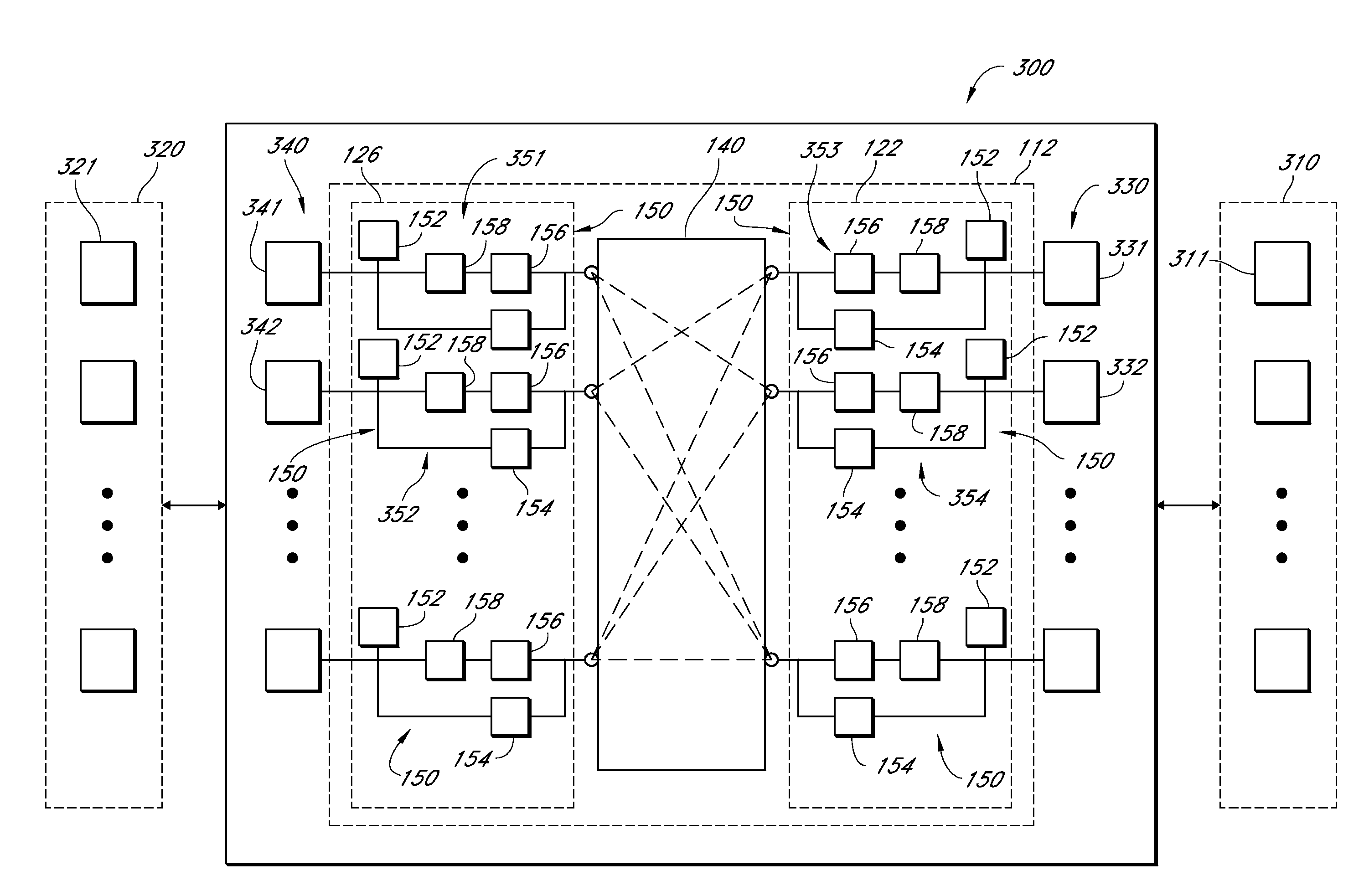
[0022]Electronic systems incorporating devices and methods in accordance with embodiments described herein may include memory subsystems that contain multiple memory boards or modules that are driven by a single memory controller which synchronizes memory access and manages memory coherency. However, having a single memory controller may gradually degrade system performance and increase power consumption as the physical and the logical size of the memory subsystem increases. Increases in memory speed may further increase the power consumption. Additionally, impedance mismatches between the system board, the memory boards, and the memory devices may also substantially degrade the performance and power efficiency of traditional memory systems. Such memory systems may be used with a power supply which helps to stabilize the voltage level, and / or a thermo-mechanical component to moderate memory subsystem temperature, and / or software for throttling the processor to lower the memory acces...


PUM


Abstract

Certain embodiments described herein include a memory module having a printed circuit board including at least one connector configured to be operatively coupled to a memory controller of a computer system. The memory module further includes a plurality of memory devices on the printed circuit board and a circuit including a first set of ports operatively coupled to at least one memory device. The circuit further includes a second set of ports operatively coupled to the at least one connector. The circuit includes a switching circuit configured to selectively operatively couple one or more ports of the second set of ports to one or more ports of the first set of ports. Each port of the first set and the second set comprises a correction circuit which reduces noise in one or more signals transmitted between the first set of ports and the second set of ports.

Description

CROSS-REFERENCE TO RELATED APPLICATIONS[0001]The present application claims the benefit of priority from U.S. Provisional Application No. 61 / 044,839, filed Apr. 14, 2008, from U.S. Provisional Application Ser. No. 61 / 044,825, filed Apr. 14, 2008, and from U.S. Provisional Application No. 61,044,801, filed Apr. 14, 2008, each of which are incorporated in their entirety by reference herein. This application is related to U.S. patent application Ser. No. 12 / 422,912, filed on even date herewith and entitled “Self-Adjusting Damper”, and to U.S. application Ser. No. 12 / 422,925, filed on even data herewith and entitled “Memory Board with Self-Testing Capability”, both of which are incorporated in their entirety by reference herein.BACKGROUND[0002]1. Field[0003]The present application relates generally to the field of electrical signal integrity and more specifically to circuits for improving electrical signal integrity.[0004]2. Description of the Related Art[0005]As the demand on the perfo...

Claims


Application Information

Patent Timeline
Patent Type & Authority Patents(United States)
IPC IPC(8): G11C5/02
CPCH05K1/0243H05K1/0216H05K2201/10189H05K2201/10159H05K2201/10053G06F13/1684G06F13/4027Y02D10/00G11C5/02G11C5/06G11C8/18
Inventor LEE, HYUNBHAKTA, JAYESH R.SOLOMON, JEFFREY C.MARTINEZ, MARIO JESUSCHEN, CHI-SHE
Owner NETLIST INC
Features
  • Generate Ideas
  • Intellectual Property
  • Life Sciences
  • Materials
  • Tech Scout
  • Unparalleled Data Quality
  • Higher Quality Content
  • 60% Fewer Hallucinations
Learn More