Light emitting apparatus

a technology of light-emitting apparatus and light-emitting resin, which is applied in the direction of electrical apparatus, semiconductor devices, solid-state devices, etc., can solve the problems of reducing reflectivity and light intensity, corroding and discoloring the frame formed from copper or aluminum, and yellowing of epoxy resin

Active Publication Date: 2012-05-08
TOYODA GOSEI CO LTD
View PDF7 Cites 2 Cited by
  • Summary
  • Abstract
  • Description
  • Claims
  • Application Information

AI Technical Summary

Benefits of technology

[0021]The light-emitting apparatus of the invention can be applied irrespective of the shape of LED, for example, a top-view type, a side-view type, a shell type, or a COB type. Moreover, the effect of the invention is particularly remarkable in light-emitting elements emitting a light having a short wavelength. Concretely, the light-emitting element such as blue color-emitting LED, purple color-emitting LED, and monochromic LED or white LED containing a fluorescent substance, which uses purple color-emitting LED can be cited. A silicone sealant is adopted owing to durability against such a light-emitting element. As the light-emitting element emitting a light having a short wavelength, a Group III nitride-based compound semiconductor light-emitting element is preferable. Herein, the Group III nitride-based compound semiconductor is represented by the general formula AlxGayIn1-x-yN (0≦X≦1, 0≦Y≦1, 0≦X+1≦1), wherein at least a part of the Group III element may be replaced by boron (B), thallium (Tl), or the like and at least a part of nitrogen (N) may be also replaced by phosphorus (P), arsenic (As), antimony (Sb), bismuth (Bi), or the like.
[0022]Moreover, the Group III nitride-based compound semiconductor may be one containing any dopant. As n-type impurities, silicon (Si), germanium (Ge), selenium (Se), tellurium (Te), carbon (C), and the like can be used. As p-type impurities, magnesium (Mg), zinc (Zn), beryllium (Be), calcium (Ca), strontium (Sr), barium (Ba), and the like can be used. In this connection, after the p-type impurity is doped, the III nitride-based compound semiconductor can be exposed to electron beam irradiation, plasma irradiation, or heating by an oven but the treatment is not essential.
[0023]The Group III nitride-based compound semiconductor layer is formed by an MOCVD (organic metal vapor phase growth) method. It is not necessary to form all the semiconductor layers constituting the element by the MOCVD method and it is possible to use a molecular beam crystal epitaxy method (MBE method), a halide-based vapor phase epitaxy method (HVPE method), a spattering method, an ion plating method, and / or the like in combination.
[0024]As the configuration of the light-emitting element, a homo-structure having an MIS junction, a PIN junction, or a pn junction, a hetero-structure, or a double hetero-structure can be adopted. It is also possible to adopt a quantum well structure (single quantum well structure or multiple quantum well structure) as a light-emitting layer. As such a Group III nitride-based compound semiconductor light-emitting element, a face-up type whose main light-receiving light-emitting direction (electrode face) is directed to a light-axis direction of the light apparatus and a flip-chip type whose main light-receiving light-emitting direction is directed to a reverse direction of the light axis and a reflected light can be adopted.
[0025]The following describes embodiments of the invention in detail while Examples thereof are compared with Comparative Examples.<Measurement of Spin-Spin Relaxation Time of Various Silicone Resins>
[0026]The spin-spin relaxation times of various silicone resins were measured under the following conditions.

Problems solved by technology

However, with the increase in light intensity of the light-emitting element, a problem that the epoxy resin is yellowed due to the heat and light from the light emitting element.
However, the inventors found a problem when a silicon resin is used as a sealant.
The problem is that a lead frame formed from a silver-plated copper base material and formed from copper or aluminum is corroded and discolored to reduce reflectivity and lower light intensity.

Method used


Image

  • Light emitting apparatus
  • Light emitting apparatus
  • Light emitting apparatus

Examples


Embodiment Construction

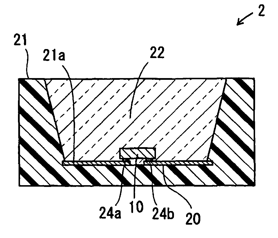
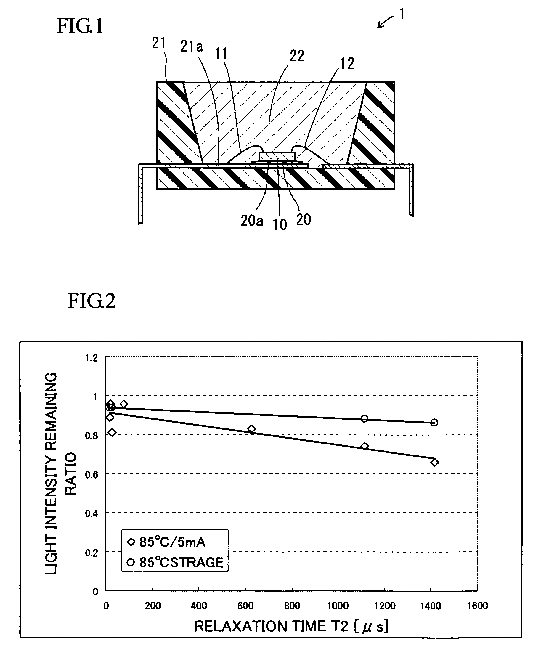
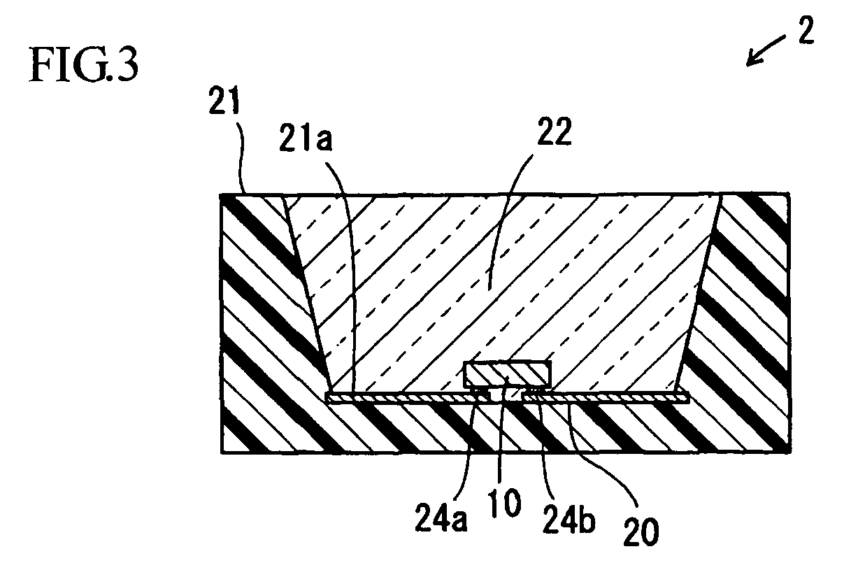
[0014]In the light-emitting apparatus of the invention, a light-emitting element is fixed to a lead frame. Also, at least a surface of the lead frame facing the light emitting element is formed from Ag, Cu, or Al as a major component. As examples of such lead frame, lead frames formed from copper, copper alloys such as brass or stainless steel as a base material which is silver plated can be cited. Also, A lead frame having a base plating like Cu plating under the silver plating. Additionally, as a lead frame without plating, lead frames formed from copper or copper alloy, or lead frames formed from Al or Al alloy can be cited. The surface of these lead frames tend to be discolored by the action of a sulfur based compound or a chlorine-based compound but, in the light-emitting apparatus of the invention, the discoloration of the lead frames can be effectively prevented over a long period of time.

[0015]Moreover, in the light-emitting apparatus of this embodiment, as the silicone resi...


PUM

PropertyMeasurementUnit
resonance frequencyaaaaaaaaaa
spin-spin relaxation timeaaaaaaaaaa

Abstract

In a light-emitting apparatus using a silicone resin as a sealant of its light-emitting element, it is intended to prevent discoloration of its lead frame. A light-emitting element fixed to a lead frame is sealed with a sealed portion formed by a silicone resin. An average spin-spin relaxation time of the silicone resin is equal to or smaller than 100 microseconds at 25° C. at a resonance frequency of 25 MHz.

Description

CROSS-REFERENCE TO RELATED APPLICATIONS[0001]This application claims priority from Japanese Patent Application JP-2008-225839 filed on Sep. 3, 2008 and the entire subject matter of which is incorporated herein by reference.TECHNICAL FIELD[0002]The present invention relates to a light-emitting apparatus including a light-emitting element sealed with a silicone resin. According to the light-emitting apparatus of the invention, discoloration of a lead frame on which the light-emitting element is mounted can be prevented.BRIEF DESCRIPTION OF RELATED ART[0003]Hitherto, a light-emitting apparatus including a light-emitting element sealed with a transparent resin is known. As the type of the transparent resin, an epoxy resin has been used in consideration of heat resistance, chemical resistance, electric insulation performance, and light transparency. However, with the increase in light intensity of the light-emitting element, a problem that the epoxy resin is yellowed due to the heat and ...

Claims


Application Information

Patent Timeline
Patent Type & Authority Patents(United States)
IPC IPC(8): H01L33/00H01L33/62H01L33/56
CPCC08L83/04C08G77/70H01L33/56H01L2224/45144H01L24/45H01L2224/32245H01L2224/48091H01L2224/48247H01L2224/73265H01L2224/85424H01L2224/85439H01L2224/85447H01L2924/00014H01L2924/00H01L2224/48624H01L2224/48639H01L2224/48647H01L2924/12036H01L2924/181H01L2924/00012
Inventor ITO, YUHKI
Owner TOYODA GOSEI CO LTD
Why Eureka
Try Eureka