Nonvolatile latch circuit

a latch circuit and non-volatile technology, applied in the field of non-volatile latch circuits, can solve the problems of increasing operating power, data and processed data potentially disappearing, and complicating power control, so as to reduce the magnetization reversal current

Active Publication Date: 2012-05-08
NEC CORP
View PDF10 Cites 10 Cited by
  • Summary
  • Abstract
  • Description
  • Claims
  • Application Information

AI Technical Summary

Benefits of technology

[0011]Therefore, an object of the present invention is to provide a technique for reducing a magnetization reversal current of a nonvolatile latch circuit having a magnetoresistive element.
[0013]The present invention effectively reduces the magnetization reversal current of a nonvolatile latch circuit having a magnetoresistive element.

Problems solved by technology

In recent years, vast numbers of logical circuits are integrated within an LSI due to the advancement of the microtechnology in the manufacture process, and this raises problems of increases in the operating power due to speeding-up and in the standby power such as leak currents.
However, this necessitates transfer of processed data to a nonvolatile storage device immediately before power-down, since initial values and intermediate processes values of data and processed data potentially disappear.
This complicates the power control and increases the costs of system components.
In addition, initial values of latch circuits and the flipflops are indefinite, and this necessitates an initializing operation of the logical circuits at power-on, disadvantageously leading to a delay of the system booting.
Furthermore, and the layout is complicated, since three kinds of power lines: main power lines, virtual power lines and ground lines are required; this makes the design using an automatic layout tool difficult.
Accordingly, the design cost is disadvantageously increased.
In a latch using a ferroelectric capacitor, however, it is difficult to integrate the latch in an interconnection layer, since a ferroelectric capacitor requires a high-temperature process in the manufacture.
Therefore, the cell area of the flipflop is undesirably increased.
In addition, the design using an automatic layout tool may be difficult, since a low-impedance plate line needs to be routed to one terminal of the ferroelectric capacitor.
However, in this latch circuit, the efficiency of generating the magnetic field by the magnetization reversal current is low and thus, a large magnetization reversal current (typically, a few miliamperes) is required.
Consequently, the size of the transistor used in a circuit for feeding the magnetization reversal current is increased, resulting in an increase in the cell area of the latch circuit.

Method used


Image

  • Nonvolatile latch circuit
  • Nonvolatile latch circuit
  • Nonvolatile latch circuit

Examples


first embodiment

(First Embodiment)

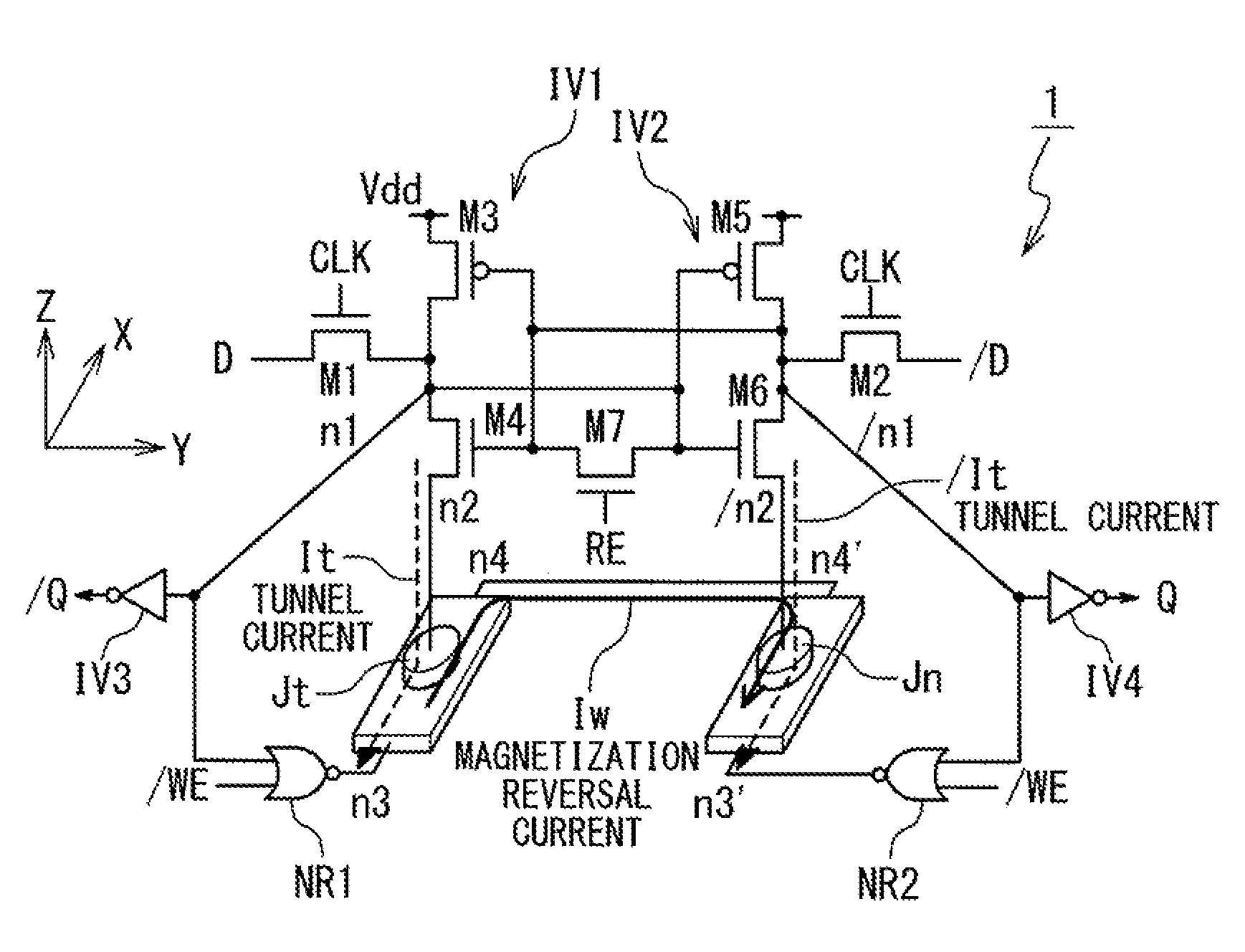
[0026]FIG. 1 is a basic configuration view illustrating a nonvolatile latch circuit 1 in a first embodiment of the present invention. The nonvolatile latch circuit 1 includes two MTJ elements Jt, Jn, NMOS transistors M1, M2, M4, M6, M7, PMOS transistors M3, M5, NOR gates NR1, NR2 and inverters IV3, IV4.

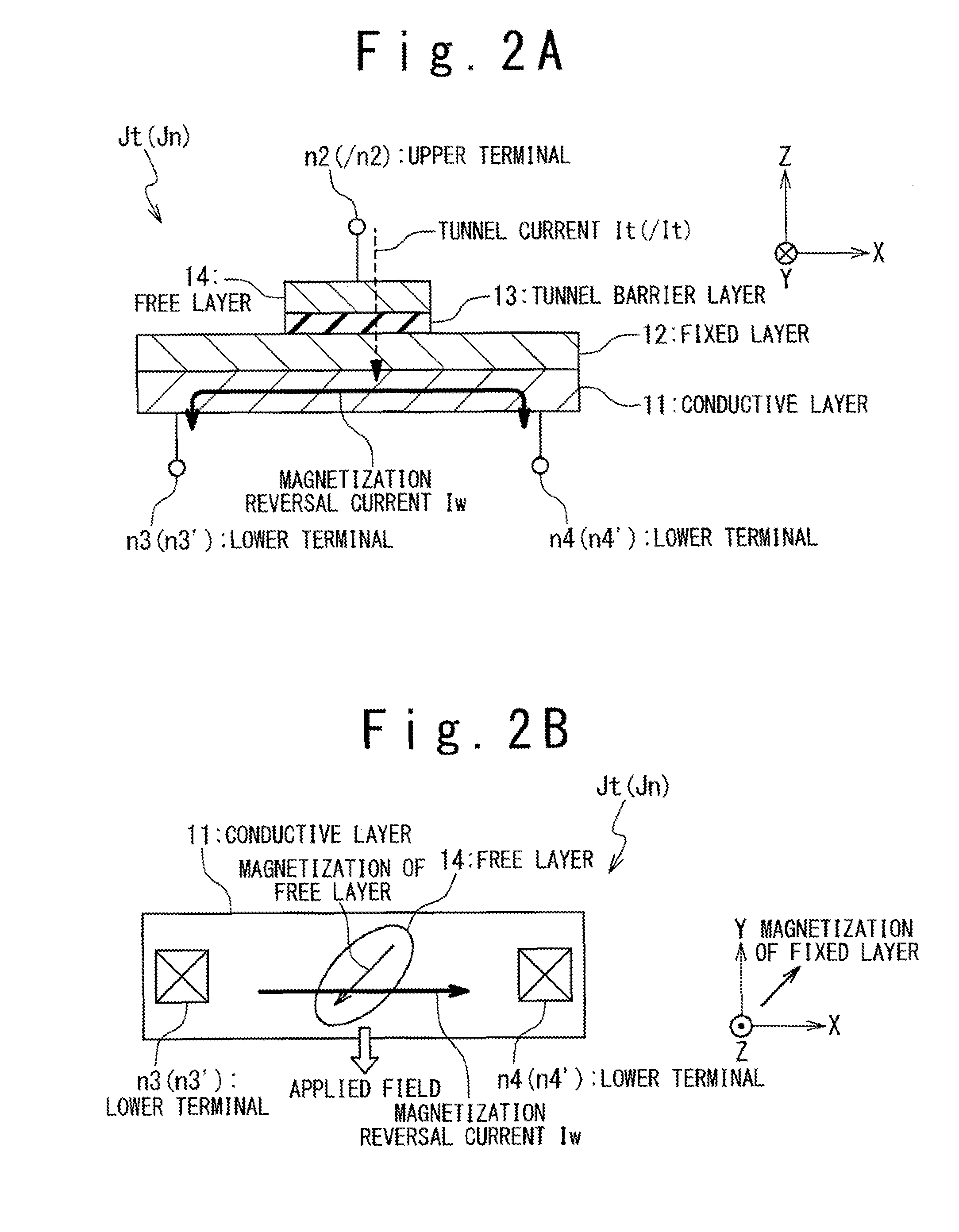
[0027]The MTJ elements Jt and Jn are used to store data in the nonvolatile latch circuit 1 when power is not supplied to the nonvolatile latch circuit 1. In this embodiment, the MTJ elements Jt and Jn are configured as a three terminal element. Specifically, the MTJ element Jt includes an upper terminal n2 and two lower terminals n3, n4, and the MTJ element Jn includes an upper terminal / n2 and two lower terminals n3′, n4′. The lower terminals n4 and n4′ of the MTJ elements Jt and Jn are connected to each other through an interconnection. As described later, a tunnel current It passing through the MTJ formed within the MTJ element Jt flows from the upper terminal n2 ...

second embodiment

(Second Embodiment)

[0054]In a second embodiment of the present invention, a nonvolatile latch circuit of the present invention is configured so as to operate as a delay flipflop (D-FF). A nonvolatile D flipflop circuit 1C in the second embodiment has a configuration in which a commonly-used master-slave typed D-FF is modified to use the high-through nonvolatile latch circuit 1 shown in FIG. 4 as a slave latch.

[0055]In detail, the nonvolatile D flipflop circuit 1C in the second embodiment includes a master latch 31, a slave latch 32 and inverters IV22 to IV24. The master latch 31 includes clocked inverters CI1, CI2 and an inverter IV21.

[0056]The clocked inverter CI1 includes PMOS transistors M21, M22, NMOS transistors M23 and M24. The input data D are supplied to the gates of the PMOS transistor M21 and the NMOS transistor M24. A non-inverted signal p1 of the clock signal CLK is inputted to the gate of the PMOS transistor M22 and the inverted signal / p1 of the clock signal CLK is inp...


PUM


Abstract

A nonvolatile latch circuit includes: first and second inverters cross-coupled to hold 1-bit data; first and second magnetoresistive elements each having first to third terminals; and a current supply circuitry configured to supply a magnetization reversal current for changing the magnetization states of the first and second maqnetoresistive elements in response to the 1-bit data. The power terminal of the first inverter is connected to the first terminal of the first magnetoresistive element and the power terminal of the second inverter is connected to the first terminal of the second magnetoresistive element. The current supply circuitry is configured to supply the magnetization reversal current to the second terminals of the first and second magnetoresistive elements. The third terminal of the first magnetoresistive element is electrically connected to the third terminal of the second magnetoresistive element.

Description

[0001]This application is the National Phase of PCT / JP2008 / 071940, filed Dec. 3, 2008, which claims the priority based on the Japanese Patent Application No. 2007-316397, filed on Dec. 6, 2007, the disclosure of which is incorporated herein in its entirety by reference.TECHNICAL FIELD[0002]The present invention relates to a nonvolatile latch circuit, and more particularly to a nonvolatile latch circuit having an MTJ (Magnetic Tunnel Junction) element as a memory element.BACKGROUND ART[0003]A lot of logical circuits are used in a large scale integration circuit (LSI). Logical circuits used in LSIs are broadly classified into logical gates which are used to process digital logical values, and typified by inverters, NAND gates and NOR gates; and bistable logical circuits used to temporarily hold and store digital logical values. Bistable logical circuits are typified by various latch circuits and various flipflop circuits formed by combining the latch circuits. In a typical LSI, combin...

Claims


Application Information

Patent Timeline
Patent Type & Authority Patents(United States)
IPC IPC(8): G11C11/00
CPCG11C11/16G11C14/0081H01L27/222H01L43/08H03K3/356008H03K3/45H01L27/11Y10S977/933Y10S977/935G11C11/18G11C11/1659G11C11/161G11C11/1675H10B10/00
Inventor SAKIMURA, NOBORUSUGIBAYASHI, TADAHIKONEBASHI, RYUSUKE
Owner NEC CORP
Why Eureka
Try Eureka