Organic memory device

a memory device and organic technology, applied in the field of semiconductor devices, can solve the problems of inability to additionally write data, increase the manufacturing steps of the device, and limit the forming method, and achieve the effects of simple structure, low cost, and simple manufacturing process

Inactive Publication Date: 2012-05-29
SEMICON ENERGY LAB CO LTD
View PDF10 Cites 4 Cited by
  • Summary
  • Abstract
  • Description
  • Claims
  • Application Information

AI Technical Summary

Benefits of technology

[0010]In view of the foregoing problems, it is an object of the present invention to overcome inhibition of element miniaturization and a complicated manufacturing process. It is another object of the present invention to provide a nonvolatile memory device in which data can be additionally written other than in manufacturing and forgery and the like due to rewriting can be prevented, and a semiconductor device including the memory device. In addition, it is also an object to provide a nonvolatile memory device and a semiconductor device which are highly reliable and inexpensive.
[0031]By the present invention, advantageous effect such as miniaturization of an element and a simplified manufacturing process can be achieved.
[0032]In addition, a memory device and a semiconductor device according to the present invention includes a memory element having a simple structure in which an organic layer is interposed between a pair of electrodes over the same insulating film, and thus, an inexpensive memory device and semiconductor device can be provided.

Problems solved by technology

A mask ROM has a simple structure; however, it is necessary to write data during manufacturing steps, and data cannot be additionally written.
An EPROM, an EEPROM, and a flash memory are nonvolatile memory circuits; however, there is a problem that manufacturing steps thereof are increased because an element having two gate electrodes is used.
However, when the electrode is formed over an organic layer, a temperature is limited because the organic layer can be influenced depending on a temperature for forming the electrode.
A forming method is limited due to this limitation of a temperature.
Therefore, there are problems that an expected electrode cannot be formed, and miniaturization of an element is inhibited.
A problem caused by an electrode formed over an organic layer is required to be solved from an aspect of inhibition of element miniaturization.
Therefore, there is a problem that a manufacturing process becomes complicated.
The complicated manufacturing process is a problem that is required to be solved from an aspect of a manufacturing cost.

Method used


Image

  • Organic memory device
  • Organic memory device
  • Organic memory device

Examples


embodiment mode 1

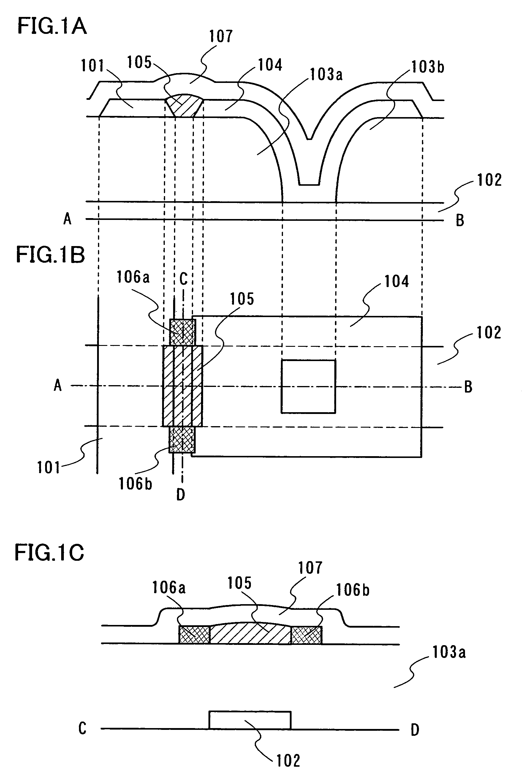
[0052]In this embodiment mode, one example of a structure of a memory element included in a semiconductor device according to the present invention will be explained with reference to the drawings. More specifically, a case where a structure of a memory circuit provided with a plurality of memory elements is a passive matrix type will be shown.

[0053]FIG. 1A shows a part of a cross-sectional structure of a memory cell array including a plurality of memory elements according to the present invention. FIG. 1B is a top structure, and a cross-section taken along a chain line A-B corresponds to FIG. 1A. Further, FIG. 1C shows a cross-sectional structure taken along a chain line C-D in FIG. 1B.

[0054]In FIG. 1A, a word line 102 is provided over a substrate having an insulated surface, and first insulating layers 103a and 103b are provided over the word line 102. The first insulating layers 103a and 103b have a film thickness of 0.8 to 1.5 μm, which is extend across the substrate surface.

[00...

embodiment mode 2

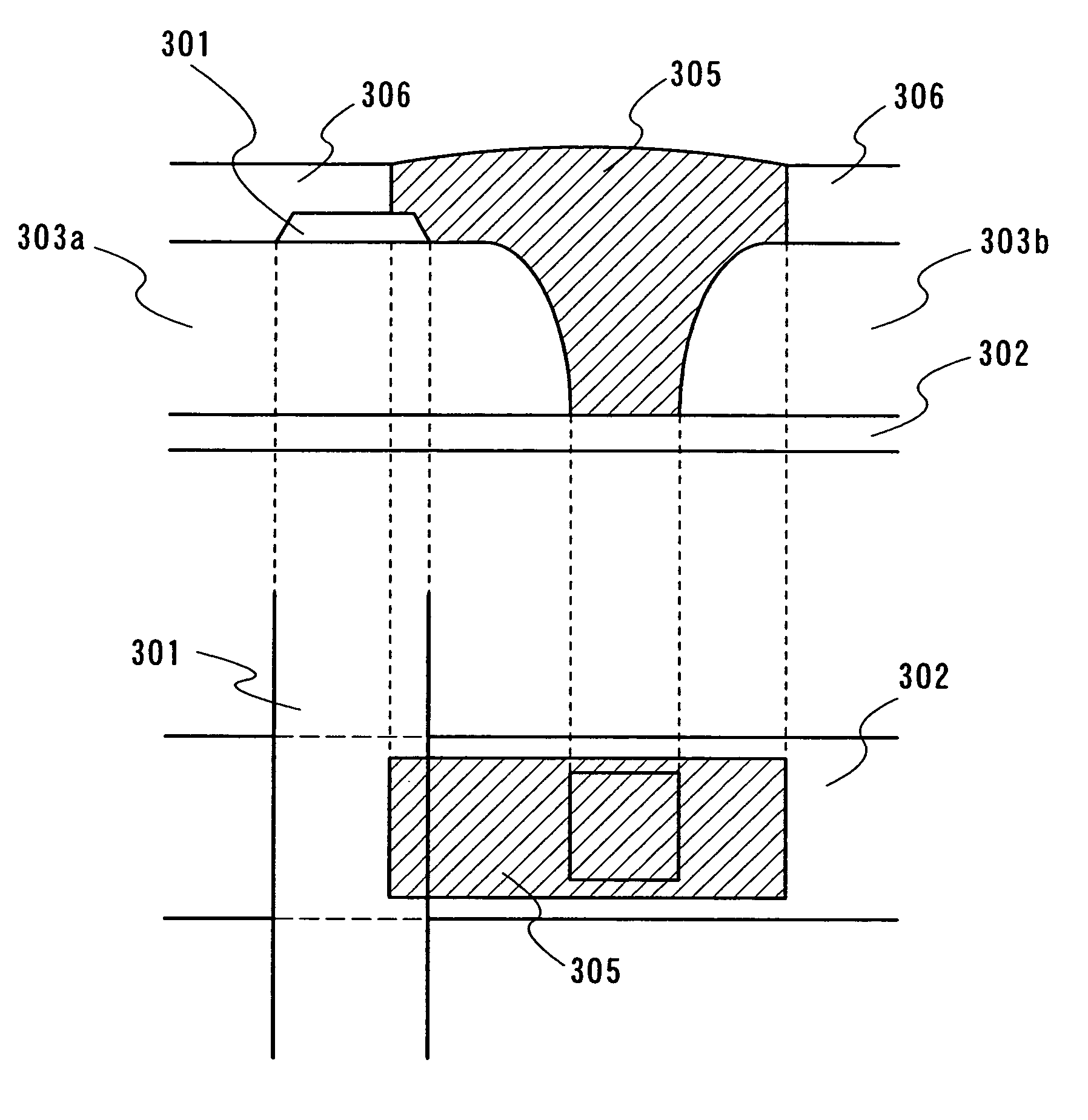
[0103]In this embodiment mode, FIGS. 3A and 3B show an example of a memory element which is partially different from the memory element shown in FIGS. 1A, 1B and 1C. FIG. 3A is a cross-sectional view of the memory element, and FIG. 3B is a top view corresponding to FIG. 3A.

[0104]In FIG. 3A, similarly to FIG. 1A, a word line 302 is provided over a substrate having an insulated surface, and first insulating layers 303a and 303b are provided over the word line 302. The first insulating layers 303a and 303b are formed by using the same material, in which an opening (a contact hole) that reaches the word line 302 is provided. A bit line 301 is provided over the first insulating layer 303a.

[0105]In FIG. 3A, the word line electrode 104 shown in FIG. 1A is not provided. Therefore, further simplification of an element structure can be achieved, and downsizing of a memory cell can also be achieved. In FIG. 3A, a layer 305 containing an organic compound is provided to cover the opening that r...

embodiment mode 3

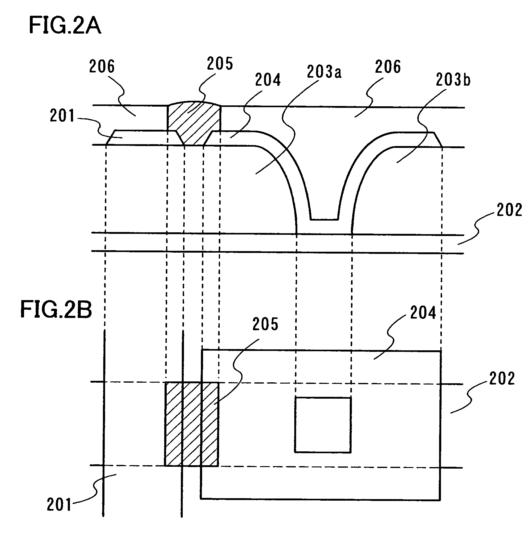
[0112]In this embodiment mode, FIGS. 4A and 4B show an example of a memory element which is partially different from the memory element shown in FIGS. 1A, 1B and 1C. FIG. 4A is a cross-sectional view of the memory element, and FIG. 4B is a top view corresponding to FIG. 4A.

[0113]In FIG. 4A, similarly to FIG. 1A, a word line 402 is provided over a substrate having an insulated surface, and first insulating layers 403a and 403b are provided over the word line 402. The first insulating layers 403a and 403b are formed by using the same material, in which an opening (a contact hole) that reaches the word line 402 is provided. A word line electrode 404 is provided so as to cover the opening. In addition, the word line electrode 404, which is electrically connected to the word line 402 through the opening, is provided over the first insulating layers 403a and 403b. The word line electrode 404 and a bit line 401 are formed in the same layer, that is, over the first insulating layer 403a.

[0...


PUM


Abstract

When an electrode is formed over an organic layer, a temperature is limited because the organic layer can be influenced depending on a temperature in forming the electrode. Therefore, there are problems that an expected electrode cannot be formed, and miniaturization of an element is inhibited. The present invention provides a structure of an organic memory element in which two electrodes are provided in the same layer as two terminals of the memory element, and a layer containing an organic compound is provided between the electrodes. By narrowing a distance between the two electrodes, writing can be performed at low voltage. In addition, a structure of the memory element is simplified, and the area of the memory element can be reduced.

Description

BACKGROUND OF THE INVENTION[0001]1. Field of the Invention[0002]The present invention relates to a semiconductor device, particularly a semiconductor device which can store data by using an organic compound for a memory circuit.[0003]In this specification, a semiconductor device generally means a device which can function by utilizing semiconductor characteristics, and an electrooptic device, a semiconductor circuit, and electronic equipment are all semiconductor devices.[0004]2. Description of the Related Art[0005]A memory element generally has a structure in which two electrodes are provided above and below a dielectric layer as two terminals of the memory element.[0006]In Patent Document 1 (Japanese Patent Laid-Open No.: 2002-26277), a memory device is proposed, in which electrodes are provided above and below an organic layer as two terminals of an element, voltage is applied to cause short-circuit, and information is stored by setting an initial state to be “0” and a conducted ...

Claims


Application Information

Patent Timeline
Patent Type & Authority Patents(United States)
IPC IPC(8): H01L51/00H01L27/28
CPCH01L27/285H01L51/0059H01L51/006H10K19/202H10K85/631H10K85/633
Inventor SATO, TAKEHISAKATO, KIYOSHI
Owner SEMICON ENERGY LAB CO LTD
Why Eureka
Try Eureka