Piezoelectric element having etched portion to form stepped recesses between layers and manufacturing method thereof, head gimbal assembly, and disk drive device with the same

a technology of etched portions and stepped recesses, which is applied in piezoelectric/electrostrictive transducers, record information storage, instruments, etc., can solve the problems of small insulation resistance, adversely affecting the ability of the read/write head to accurately read data from and write data to the disk, and becoming more and more difficult to quickly and accurately position the read/write head over the desired information tracks on the disk. , to achieve the effect of high insulation resistan

Inactive Publication Date: 2012-06-05
SAE MAGNETICS (HK) LTD
View PDF2 Cites 40 Cited by
  • Summary
  • Abstract
  • Description
  • Claims
  • Application Information

AI Technical Summary

Benefits of technology

[0011]Accordingly, an object of the present invention is to provide a piezoelectric element which possesses higher insulation resistance.
[0012]Another object of the present invention is to provide a method of manufacturing a piezoelectric element. The method could not only manufacture a piezoelectric element with higher insulation resistance, but also manufacture the piezoelectric element with low reject rate and low manufacture cost.
[0013]Another object of the present invention is to provide a head gimbal assembly with a piezoelectric element, the piezoelectric element of the head gimbal assembly possesses higher insulation resistance and a better operation performance.
[0014]Still another object of the present invention is to provide a disk drive unit, a piezoelectric element of the disk drive unit possesses higher insulation resistance and a better operation performance.
[0027]In comparison with the prior art, the side surfaces of the first and the second laminated structure bodies of the piezoelectric element that are parallel to the laminating direction both have at least a portion etched to form a recess so that a step distance is formed between sides of the two adjacent electrode layers that are parallel to the laminating direction. Therefore, compared with the aligned up-and-down sides of the two adjacent electrodes, the present invention increases insulation resistance between two adjacent electrodes on the opposite surfaces of the piezoelectric layer, which in turn, reduces reject rate of the piezoelectric element and lowers manufacture cost. In addition, because the first and the second laminated structure bodies are symmetrically laminated and bonded together, the piezoelectric element has a sound force balancing performance, which further optimizes mechanical performance of the piezoelectric element. Besides, the recesses of the first and the second laminated structure bodies are filled with insulation resin therein, which further increases insulation resistance between the two adjacent electrode layers on the opposite surfaces of the piezoelectric layer.

Problems solved by technology

As track density increases, it becomes more and more difficult to quickly and accurately position the read / write head over the desired information tracks on the disk.
However, because the inherent tolerances of the VCM 105 and the HGA 106 exist in the displacement of the slider 103 by employing VCM 105 alone, the slider 103 cannot achieve quick and fine position control which adversely impacts the ability of the read / write head to accurately read data from and write data to the disk 101.
However, the PZT element 120a / 120b manufactured by above-mentioned method has a small insulation resistance, a high reject rate and a high manufacture cost.
The same problems also occur in the second electrode-piezoelectric combination structure.

Method used


Image

  • Piezoelectric element having etched portion to form stepped recesses between layers and manufacturing method thereof, head gimbal assembly, and disk drive device with the same
  • Piezoelectric element having etched portion to form stepped recesses between layers and manufacturing method thereof, head gimbal assembly, and disk drive device with the same
  • Piezoelectric element having etched portion to form stepped recesses between layers and manufacturing method thereof, head gimbal assembly, and disk drive device with the same

Examples


first embodiment

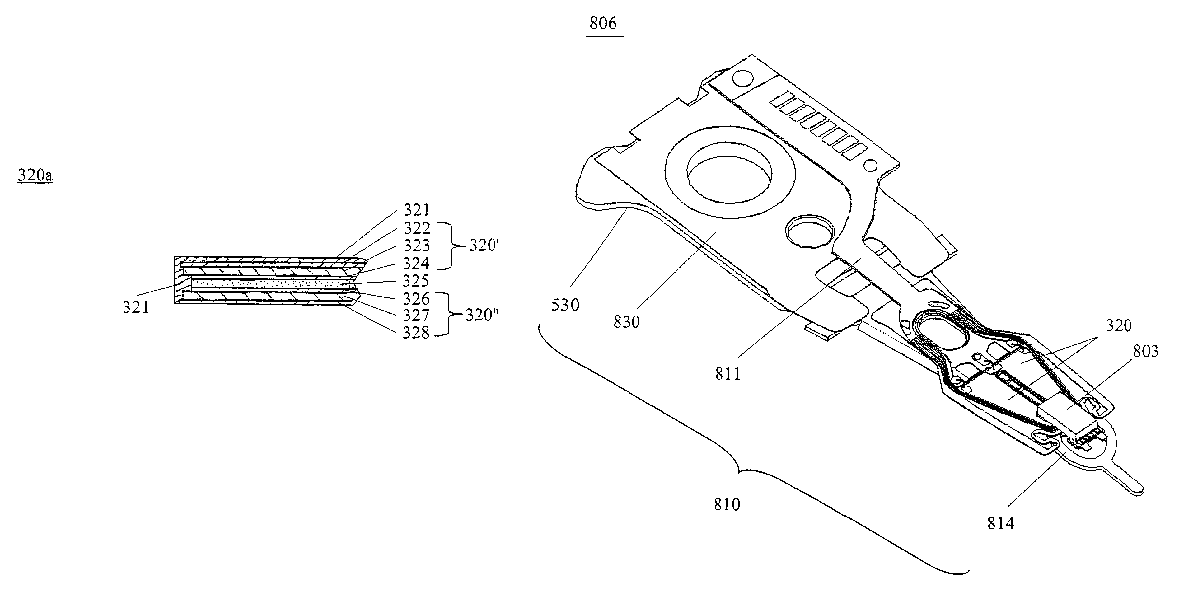
[0048]Various preferred embodiments of the invention will now be described with reference to the figures, wherein like reference numerals designate similar parts throughout the various views. FIG. 4a is a sectional view of a piezoelectric element 320a according to the present invention. FIG. 4b is a sectional view of inner structure of the piezoelectric element 320a of FIG. 4a. As shown, the piezoelectric element 320a comprises a first laminated structure body 320′ and a second laminated structure body 320″. The first and the second laminated structure bodies 320′, 320″ are both laminated by electrode layer and piezoelectric layer alternately to define a laminating direction, and each piezoelectric layer is sandwiched between two adjacent electrode layers.

[0049]The first laminated structure body 320′ comprises a first piezoelectric layer 323, a first electrode layer 322 and a second electrode layer 324 which are positioned on two opposite surfaces of the first piezoelectric layer 32...

second embodiment

[0055]FIG. 8a is a sectional view of a piezoelectric element 420 according to the present invention. As shown, the piezoelectric element 420a comprises a laminated structure body and the laminated structure body is laminated by electrode layer and piezoelectric layer alternately to define a laminating direction, and each piezoelectric layer is sandwiched between two adjacent electrode layers. Specifically, the laminated structure body comprises a piezoelectric layer 423, a first electrode layer 422 and a second electrode layer 424 which are positioned on two opposite surfaces of the piezoelectric layer 423. Side surface of the laminated structure body that is parallel to the laminating direction has a portion etched to form a recess so that a step distance D41 is formed between sides of the two adjacent electrode layers 422, 424 that are parallel to the laminating direction. The step distance D41 is preferably 10 micrometers. In the subject embodiment, the side surface is etched int...

third embodiment

[0056]FIG. 8b is a sectional view of a piezoelectric element 520 according to the present invention. As shown, the piezoelectric element 520a comprises a laminated structure body and the laminated structure body is laminated by electrode layer and piezoelectric layer alternately to define a laminating direction, and each piezoelectric layer is sandwiched between two adjacent electrode layers. Specifically, the laminated structure comprises a piezoelectric layer 523, a first electrode layer 522 and a second electrode layer 524 which are positioned on two opposite surfaces of the piezoelectric layer 523. Side surface of the laminated structure body that is parallel to the laminating direction has a portion etched to form a recess so that a step distance D51 is formed between sides of the two adjacent electrode layers 522, 524 that are parallel to the laminating direction. The step distance D51 is preferably 10 micrometers. In the subject embodiment, the side surface is etched into inc...


PUM

PropertyMeasurementUnit
step distanceaaaaaaaaaa
step distance D41aaaaaaaaaa

Abstract

A piezoelectric element comprises a first laminated structure body and a second laminated structure body. Side surfaces of the first and the second laminated structure bodies that are parallel to a laminating direction both have at least a portion etched to form a recess so that a step distance is formed between sides of the two adjacent electrode layers that are parallel to the laminating direction. The design of the step distance increases insulation resistance between the two adjacent electrode layers on the opposite surfaces of the piezoelectric layer, and lowers reject rate. The first and the second laminated structure bodies are symmetrically laminated and bonded together, thus optimizing force balancing performance. The present invention also discloses a method of manufacturing a PZT element, a HGA with the PZT element and a disk drive unit having such HGA.

Description

FIELD OF THE INVENTION[0001]The present invention relates to an information recording disk drive device, and more particularly, to a piezoelectric (PZT) element of the information recording disk drive device and manufacturing method of the PZT element, a head gimbal assembly (HGA), and a disk drive device.BACKGROUND OF THE INVENTION[0002]Disk drives are information storage devices that use magnetic media to store data and a movable read / write head positioned over the magnetic media to selectively read data from and write data to the magnetic media.[0003]Consumers are constantly desiring greater storage capacity for such disk drive devices, as well as faster and more accurate reading and writing operations. Thus, disk drive manufacturers have continued to develop higher capacity disk drives by, for example, increasing the recording and reproducing density of the information tracks on the disks by using a narrower track width and / or a narrower track pitch. However, each increase in tr...

Claims


Application Information

Patent Timeline
Patent Type & Authority Patents(United States)
IPC IPC(8): G11B5/56H01L41/22
CPCG11B5/5552Y10T29/42
Inventor YAO, MINGGAOSUN, YU
Owner SAE MAGNETICS (HK) LTD
Why Eureka
Try Eureka