Thin film field effect transistor

a field effect transistor and thin film technology, applied in the direction of basic electric elements, electrical equipment, semiconductor devices, etc., can solve the problems of difficult to form transistors directly on resin substrates, generally low heat resistance, etc., and achieve excellent drive durability and drive stability, and high heat resistance.

Active Publication Date: 2012-06-19
SAMSUNG DISPLAY CO LTD
View PDF7 Cites 553 Cited by
  • Summary
  • Abstract
  • Description
  • Claims
  • Application Information

AI Technical Summary

Benefits of technology

[0052]JP-A Nos. 2007-73701, 2008-42088, and 2007-123702 neither disclose nor suggest durability of TFT against heat, oxygen, ultraviolet rays, or the like.
[0053]The invention provides a TFT that employs an amorphous oxide semiconductor for an active layer, and is excellent in drive durability and drive stability. In particular, the invention provides a TFT which has excellent drive durability and drive stability by suppressing a variation of a threshold voltage during continuous driving, and shifting a voltage threshold which has been distorted toward the negative side to the positive side. Further, the invention provides a TFT that has a higher durability against heat, oxygen, ultraviolet rays, or the like in a process after production of the TFT, and is stable in electrical characteristics of the TFT without changing even aging or heating of the TFT, and a TFT in which a malfunction due to light of short wavelength such as blue light, X-rays or the like, is retarded.1. TFT
[0054]The TFT of the invention is an active element which includes at least a gate electrode, a gate insulating layer, an active layer, a source electrode, and a drain electrode in this order, and has a function of controlling the electric current that passes through the active layer when a voltage is applied to the gate electrode, and switching an electric current between the source electrode and the drain electrode. As a TFT structure, either of a staggered structure or an inverted-staggered structure may be formed.
[0055]The TFT of the invention includes, on a substrate, at least a gate electrode, a gate insulating layer, an active layer, a source electrode and a drain electrode, wherein the active layer comprises an amorphous oxide semiconductor containing at least In and Zn, a first interface layer comprising an amorphous oxide semiconductor containing Ga or Al is disposed between the gate insulating layer and the active layer such that it is adjacent to at least the active layer, the content of Ga or Al in the amorphous oxide semiconductor of the first interface layer being higher than the content of Ga or Al in the amorphous oxide semiconductor of the active layer, and a second interface layer comprising an amorphous oxide semiconductor containing Ga or Al is disposed such that it is adjacent to the active layer on the opposite side of the active layer with respect to the first interface layer, the content of Ga or Al in the amorphous oxide semiconductor of the second interface layer being higher than the content of Ga or Al in the amorphous oxide semiconductor of the active layer.
[0056]Conventionally, a top gate structure (a staggered structure) and a bottom gate structure (an inverted-staggered structure) have been known as structures of TFT in accordance with the relation of placement of a source electrode, a drain electrode and a gate electrode. Further, a top contact structure and a bottom contact structure have also been known as structures of TFT in accordance with the relation of placement of a source electrode, a drain electrode and an active layer. Any embodiment of these structures may be applied in a TFT of the present invention. For example, structures shown in FIG. 1 and FIG. 2 each belong to a staggered structure. A structure shown in FIG. 1 is a top contact structure, in which an active layer 4 is formed before a source electrode 5-1 and drain electrode 5-2 are formed. A structure shown in FIG. 2 is a bottom contact structure, in which a source electrode 5-21 and drain electrode 5-22 are formed before an active layer 24 is formed.
[0057]In a point of view of attaining high electric field effect mobility as an active layer, the amorphous oxide semiconductor of the active layer preferably contains In at a content of 70% or more and Zn at a content of 5% or more with respect to all the metal components in the amorphous oxide semiconductor of the active layer. More preferably, the content of In is 75% or more and the content of Zn is 5% or more, and still more preferably the content of In is 80% or more and the content of Zn is 5% or more. The definition with respect to the contents of In and Zn in the present invention is based on an atomic %.

Problems solved by technology

However, fabrication of the transistors using the silicon thin films described above requires a thermal treatment process at a relatively high temperature, and it is difficult to form the transistors directly on a resin substrate which is generally low in heat resistance.

Method used


Image

  • Thin film field effect transistor
  • Thin film field effect transistor
  • Thin film field effect transistor

Examples


example 1

Fabrication of TFT Element 1 of the Invention

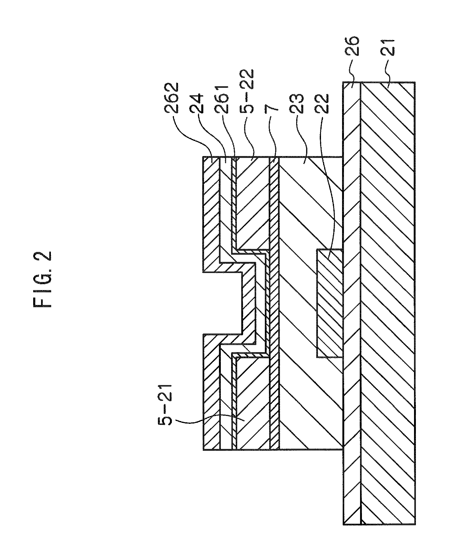
[0140]TFT element 1 of the invention having a configuration shown in FIG. 2 was fabricated as follows.

[0141]Substrate 21: a polyethylene naphthalate (PEN) film having a thickness of 125 μm was used.

[0142]Insulating layer 26: SiON was deposited to give a thickness of 500 nm by a sputtering deposition method.

[0143]Gate electrode 22: a molybdenum layer having a thickness of 40 nm was formed by a sputtering deposition method, which was subjected to photolithography and etching to form a stripe-shaped gate electrode.

[0144]Gate insulating layer 23: an acrylic resin was spin-coated, which was sintered to form a gate insulating layer 23 having a thickness of 0.5 μm.

[0145]Intermediate layer 7: on the gate insulating layer 23, an intermediate layer 7 having a thickness of 20 nm was provided by performing sputtering deposition of SiO2 through a metal mask at room temperature.

[0146]Source electrode 5-21 and drain electrode 5-22: on the whole surface ...

example 2

Fabrication of TFT Element 2 of the Invention

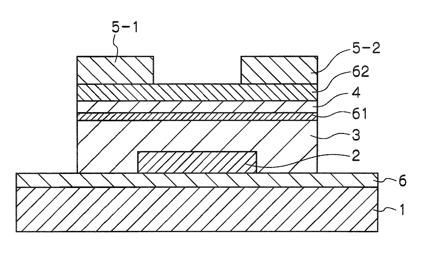
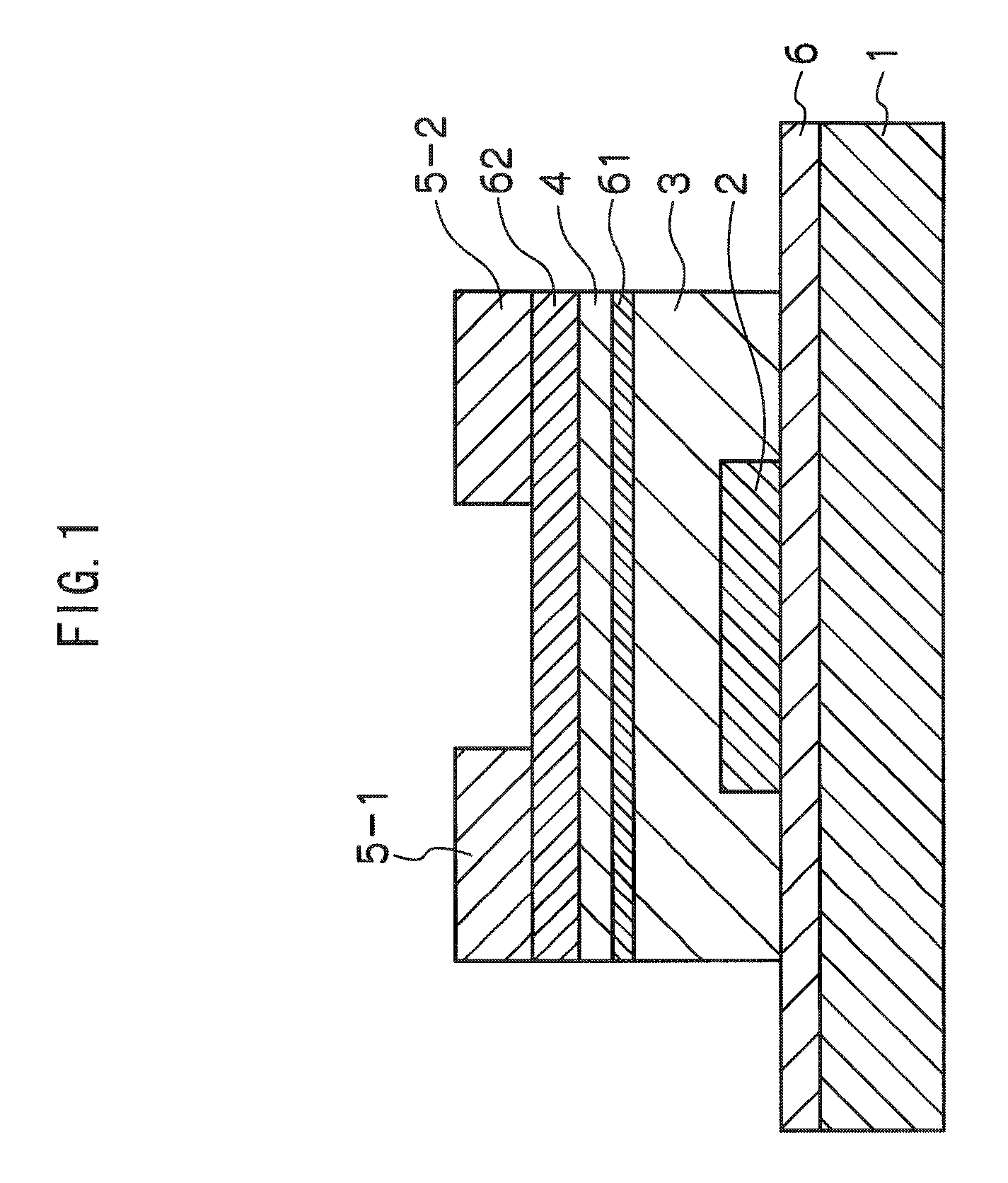
[0163]TFT element 2 of the invention having a configuration as shown in FIG. 1 was fabricated as follows.

[0164]Substrate 1: non-alkali glass having a thickness of 700 μm was used.

[0165]Gate electrode 2: a molybdenum layer having a thickness of 40 nm was formed by a sputtering deposition method, which was subjected to photolithography and etching to form a stripe-shaped gate electrode.

[0166]Gate insulating layer 3: SiO2 was formed by a sputtering deposition method at room temperature, thereby forming a gate insulating layer having a thickness of 200 nm.

[0167]First interface layer 61: on the gate insulating layer, a first interface layer having a thickness of 2.5 nm was provided by performing oxygen-introduced RF magnetron sputtering using a target having a composition of InGaZnO4 (hereinafter also referred to as “IGZO”) through a metal mask at room temperature to form an IGZO film.

[0168]Semiconductor layer (active layer) 4: on the first in...

example 3

Fabrication of TFT Element 3 of the Invention

[0171]In a similar manner to that in Example 2, a gate electrode, a gate insulating layer, and a first interface layer were successively formed on a non-alkali glass substrate.

[0172]First semiconductor layer: on the first interface layer, a first semiconductor layer having a thickness of 1.25 nm was provided by performing oxygen-introduced DC magnetron sputtering using a target having a composition of In3O2 including 10% by weight of ZnO (hereinafter also referred to as “IZO”) through a metal mask at room temperature to form an IZO film.

[0173]Intermediate interface layer: on the first semiconductor layer, an intermediate interface layer having a thickness of 2.5 nm was provided by performing oxygen-introduced RF magnetron sputtering using a target having a composition of IGZO through a metal mask at room temperature to form an IGZO film.

[0174]Second semiconductor layer: on the intermediate interface layer, a second semiconductor layer hav...


PUM


Abstract

A thin film field effect transistor has at least a gate electrode 2, a gate insulating layer 3, an active layer 4, a source electrode 5-1 and a drain electrode 5-2 on a substrate 1. The active layer includes an amorphous oxide semiconductor including at least In and Zn, a first interface layer 61 is disposed between the gate insulating layer and the active layer such that it is adjacent to at least the active layer, and a second interface layer is disposed on the opposite side of the active layer with respect to the first interface layer such that it is adjacent to the active layer. A content of Ga or Al in the amorphous oxide semiconductor of each of the first interface layer and the second interface layer is higher than a content of Ga or Al in the amorphous oxide semiconductor of the active layer.

Description

CROSS-REFERENCE TO RELATED APPLICATION[0001]This application claims priority under 35 USC 119 from Japanese Patent Application Nos. 2008-208978 filed on Aug. 14, 2008 and 2009-159841 filed on Jul. 6, 2009, the disclosures of which are incorporated by reference herein.BACKGROUND OF THE INVENTION[0002]1. Field of the Invention[0003]The present invention relates to a thin film field effect transistor in which an amorphous oxide semiconductor is used for an active layer.[0004]2. Description of the Related Art[0005]In recent years, flat panel displays (FPDs) have been put to practical use, due to the progress made in liquid crystal and electroluminescence (EL) technologies, etc. Especially, an organic electroluminescence element (hereinafter referred to as “organic EL element” in some cases) formed using a thin film material which emits light by excitation due to application of electric current can provide light emission of high brightness at low voltage, and thus is expected to achieve ...

Claims


Application Information

Patent Timeline
Patent Type & Authority Patents(United States)
IPC IPC(8): H01L29/12
CPCH01L29/7869H01L29/78696
Inventor IMAI, SHINJI
Owner SAMSUNG DISPLAY CO LTD
Why Eureka
Try Eureka