Quantitative evaluation device of atomic vacancies existing in silicon wafer, method for the device, silicon wafer manufacturing method, and thin-film oscillator

a technology of atomic vacancies and quantitative evaluation, which is applied in the direction of semiconductor/solid-state device testing/measurement, instruments, specific gravity measurement, etc., can solve the problems of difficult mass-producing wafers, difficult to mass-produce wafers, and long time for depositing zno thin films, etc., to achieve short time, short time, and efficient manufacturing

Inactive Publication Date: 2012-07-10
NIIGATA UNIVERSITY
View PDF8 Cites 3 Cited by
  • Summary
  • Abstract
  • Description
  • Claims
  • Application Information

AI Technical Summary

Benefits of technology

[0016]With the view of the above problems, it is an object of the present invention to provide a quantitative evaluation device of an atomic vacancy capable of efficiently and quantitatively evaluating an atomic vacancy existing in a silicon wafer and further to provide a quantitative evaluation method for the same.
[0039]According to the thin film oscillator of the eleventh aspect, as compared to the conventional oscillator formed with the ZnO thin film made by using a physical vapor-deposition method, the thin film oscillator is made up of a high-polymer material and thereby, a uniform thin-film can be formed with dramatic ease and within a short period of time and hence, an atomic vacancy existing in a silicon wafer can be effectively and quantitatively evaluated.

Problems solved by technology

In general, if the ZnO thin film oscillator is made by, for example, a sputtering method, it takes a long time to deposit the ZnO thin film.
According to the conventional arts, therefore, it takes a long period of time to form a transducer and hence it becomes difficult to mass-produce wafers within a short period of time and then evaluate the large quantity, in order to meet the increasing demand.
This difficulty roots in essential shortcoming of the conventional arts that a prolonged time is required for forming a good-quality ZnO thin film, and hence, it poses an unavoidable problem as long as the ZnO thin film is employed.
As for a sputtering method, a sputtering device is generally expensive and requires a high vacuum, leading to the necessity for a complicated manufacturing process.
Accordingly, for the above reasons, when using the conventional method for forming a thin film oscillator by using the sputtering method, the quantitative evaluation of an atomic vacancy existing in the silicon wafer was difficult to perform efficiently.

Method used


Image

  • Quantitative evaluation device of atomic vacancies existing in silicon wafer, method for the device, silicon wafer manufacturing method, and thin-film oscillator
  • Quantitative evaluation device of atomic vacancies existing in silicon wafer, method for the device, silicon wafer manufacturing method, and thin-film oscillator
  • Quantitative evaluation device of atomic vacancies existing in silicon wafer, method for the device, silicon wafer manufacturing method, and thin-film oscillator

Examples


examples

[0114]Next is a description of examples according to the present invention. First, as shown in FIG. 8(a), a substrate sample 57 was made by laminating a Ti thin film 56 into 200 mm in thickness on an Sb-doped N-type Si substrate 55 (its resistivity is 0.02 Ω·cm). Then, the substrate sample 57 was divided, as shown in FIG. 8(b) to obtain two or more 20 mm-square sample chips 58.

[0115]A thin film oscillator 31 formed on each of sample chips 58 from P (VDF / TrFE) by using an application method was laminated, as shown in FIG. 9. Then, six samples 59 of the thin film oscillator 31 were prepared by forming each of the film's thickness into 2, 4, 6, 8, 10 and 12 μm. In addition, by using a vapor-deposition method, each of the thus obtained samples 59 was formed with Al electrodes positioned at regular intervals as shown in FIG. 10.

[0116]Then, as shown in FIG. 11, the Si substrate 55 and each of the Al electrodes 60 were electrically connected to apply an orientation treatment to the sample ...


PUM

PropertyMeasurementUnit
thicknessaaaaaaaaaa
temperaturesaaaaaaaaaa
thicknessaaaaaaaaaa

Abstract

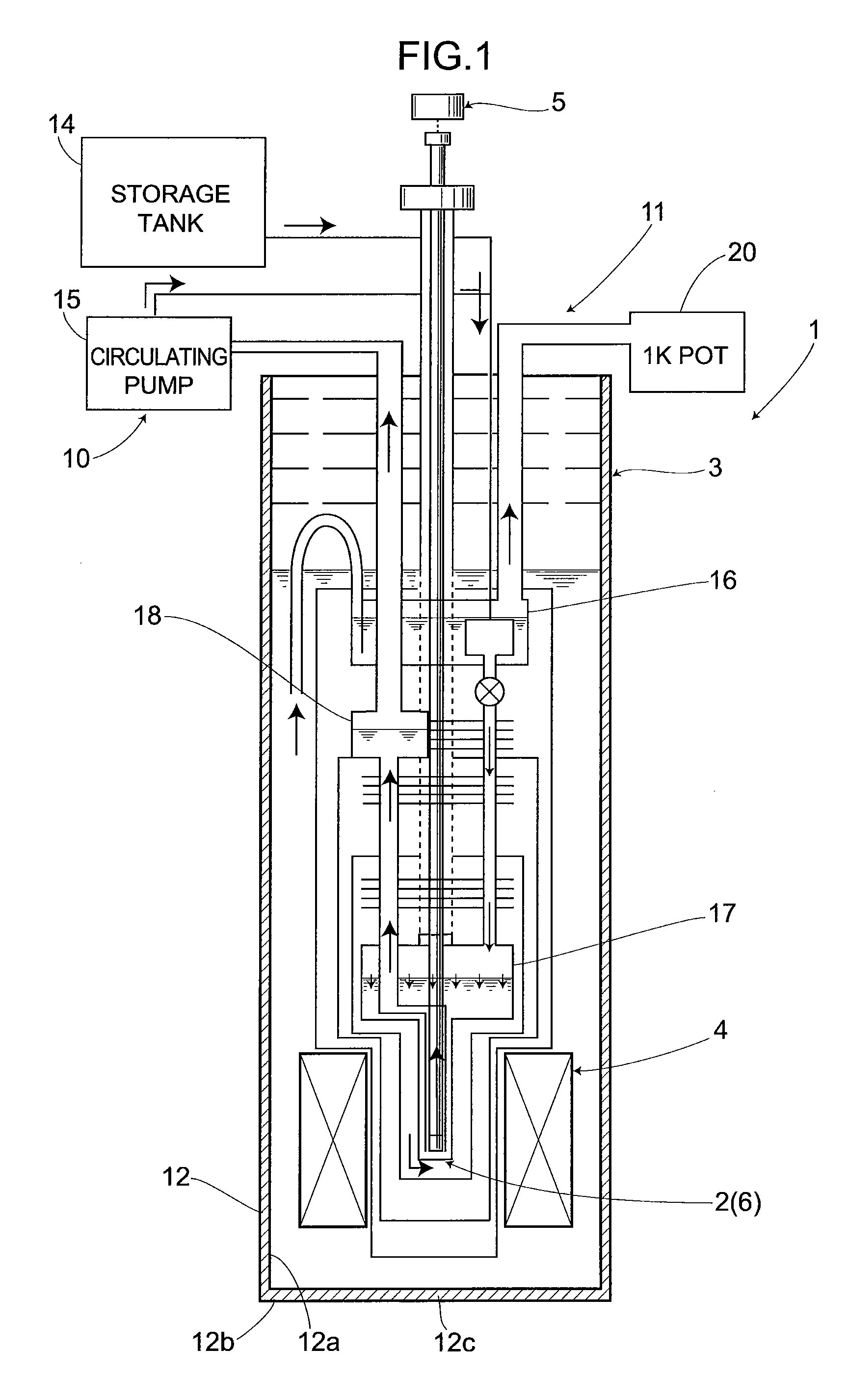
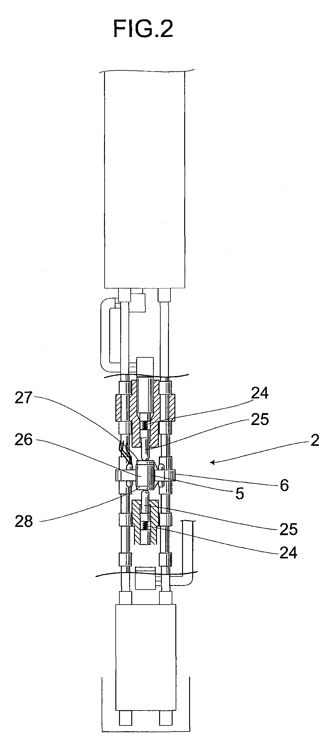
A quantitative evaluation device and method of an atomic vacancy, which are capable of efficiently and quantitatively evaluating an atomic vacancy existing in a silicon wafer. A quantitative evaluation device 1 is equipped with a detector 5 including an ultrasonic generator 27 and an ultrasonic receiver 28, a silicon sample 6 formed with the ultrasonic generator 27 and the ultrasonic receiver 28 on a silicon wafer 26 comprising perfect crystal silicon, a magnetic force generator 4 for applying an external magnetic field to the silicon sample 6, and a cooler 3 capable of cooling and controlling the silicon sample 6 to a range of temperatures lower than or equal to 50K. The ultrasonic generator 27 and the ultrasonic receiver 28 are each equipped with a transducer 30 including a thin film oscillator 31 formed from a high-polymer material with a physical property capable of following an expanding action of a silicon wafer 26 in association with a temperature drop in the above range of the temperatures and whose molecular axes are oriented in the direction of an electric field when decreasing temperature with the electric field applied thereto and further, including electrodes 32, 33 for applying an electric field to the thin film oscillator 31.

Description

CROSS-REFERENCE TO PRIOR APPLICATION[0001]This is the U.S. National Phase Application under 35 U.S.C. §371 of International Patent Application No. PCT / JP2008 / 061987 filed Jul. 2, 2008, which claims the benefit of Japanese Patent Application No. 2007-175679 filed Jul. 3, 2007, and Japanese Patent Application No. 2008-093276 filed Mar. 31, 2008, all of which are entirely incorporated by reference herein. The International Application published in Japanese on Jan. 8, 2009 as WO 2009 / 005087 A1 under PCT Article 21(2).TECHNICAL FIELD[0002]The present invention relates to a quantitative evaluation device and method of atomic vacancies existing in a silicon wafer, which are capable of direct and quantitative evaluation of a type and concentration of atomic vacancies existing in a silicon wafer manufactured by means of the Czochralski method (CZ method) or the float-zone method (FZ method) employed in the semiconductor industry.BACKGROUND[0003]Recently, a semiconductor element (LSI: Large S...

Claims


Application Information

Patent Timeline
Patent Type & Authority Patents(United States)
IPC IPC(8): G01N29/07
CPCH01L22/12G01N29/075G01N2291/02827G01N2291/0289
Inventor GOTO, TERUTAKAKANETA, HIROSHINEMOTO, YUICHI
Owner NIIGATA UNIVERSITY
Why Eureka
Try Eureka