Method for quantitative analysis of a material

a quantitative analysis and material technology, applied in the field of quantitative analysis of materials, can solve the problems of x-ray spectrum not being able to correct for feature size, method based on backscattered electrons described by u.s. pat. no. 4,559,450, and energy electron scattering within the specimen and affecting the quality of material, so as to achieve a fast and yet simple method

Active Publication Date: 2012-07-17
OXFORD INSTR NANOTECH TOOLS
View PDF15 Cites 7 Cited by
  • Summary
  • Abstract
  • Description
  • Claims
  • Application Information

AI Technical Summary

Benefits of technology

[0014]In our invention, rather than use the total BE signal, we use a detector with energy filtering so that only electrons that have lost a small fraction of their energy are detected. Electrons that are backscattered out of the specimen in the early stage of the electron trajectory near the surface will have energies close to the primary beam energy and are thus “low loss electrons” (LLEs). These LLEs produce a signal that arises from a shallow region that is close to the incident beam. For example, if incident electrons at 15 keV strike a pure Si specimen, then most electrons that have lost less than 500 eV in energy will emerge from depths and spatial extent of the order of 100 nm. Therefore, by using energy filtering, the LLE signal can be representative of much smaller objects than the total BE signal and there is no need to use a look up table to correct for the size of the object and no need to compensate for the effect of the substrate.
[0026]For example, if a candidate material has three elements, each of which is also identified in the x-ray data, then this may be given a ranking of “3”. If only two such elements are found within the x-ray data then a ranking of “2” is awarded, and so on. This therefore provides a faster and yet more simple method of selecting a set of candidate materials using the LLE data and x-ray data.

Problems solved by technology

One of the problems of analysis with electrons is that energetic electrons scatter within the specimen and penetrate below the surface.
Therefore, the method based on backscattered electrons described by U.S. Pat. No. 4,559,450 would typically not be suitable to analyse objects much smaller than 1000 nm in dimension using 15 keV incident electrons.
Consequently, the resulting x-ray spectrum cannot be corrected for feature size using a table of correction factors and there is no provision for identifying chemical elements in U.S. Pat. No. 6,753,525.
However, if the substrate were changed, the lookup table relating BE signal to object dimensions would have to be modified to compensate for the different electron scattering properties of a substrate other than silicon, this requiring significant additional effort.
The energy dependence of detectors, variation in offset current and variation in gain make characterisation of materials by backscattered electrons difficult in practice.
There are therefore a number of problems associated with the use of backscattered electrons and x-ray techniques in obtaining compositional information, particularly where analysis is needed of objects having small dimensions, such as less than 1000 nanometres.

Method used


Image

  • Method for quantitative analysis of a material
  • Method for quantitative analysis of a material
  • Method for quantitative analysis of a material

Examples


example 1

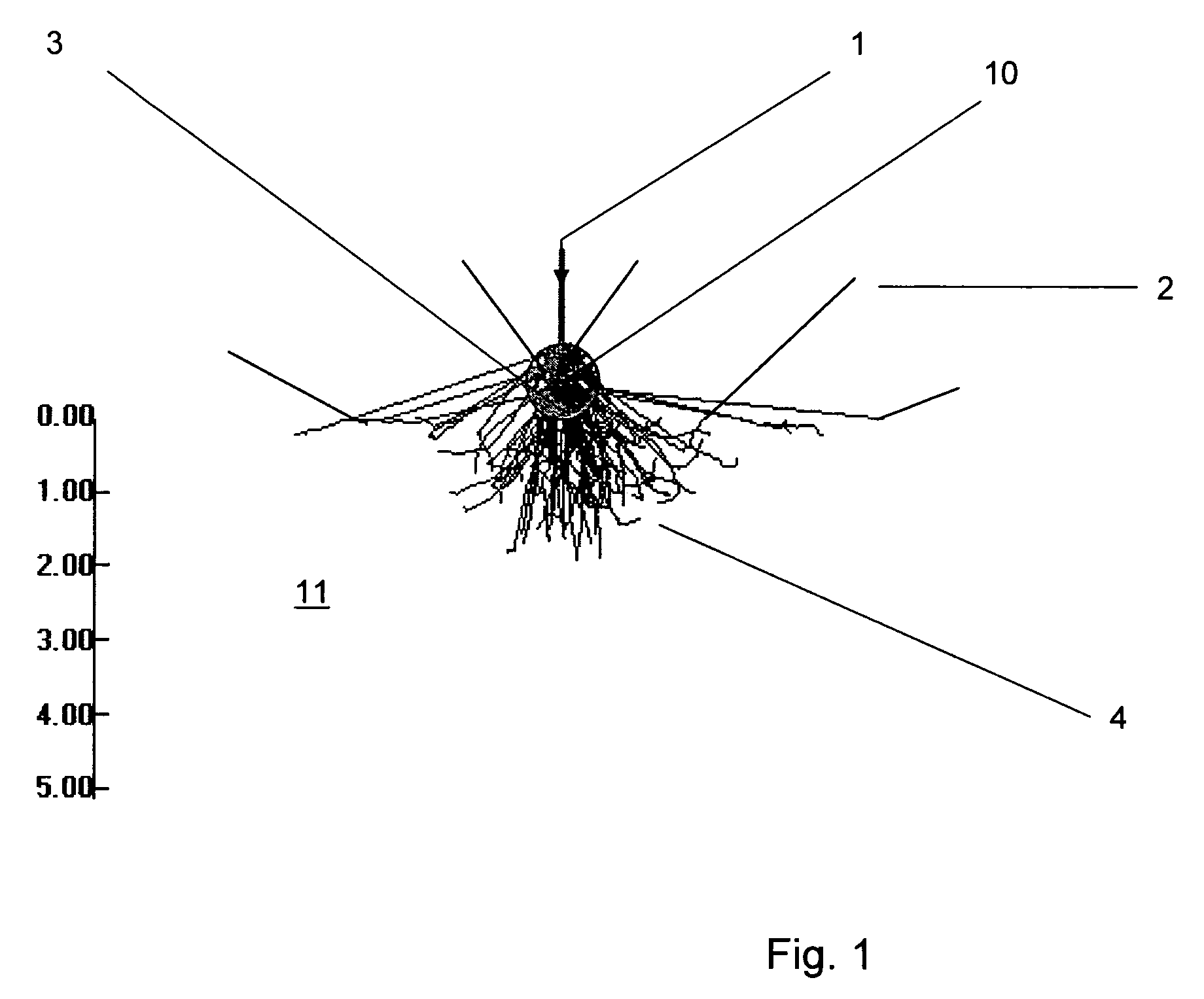
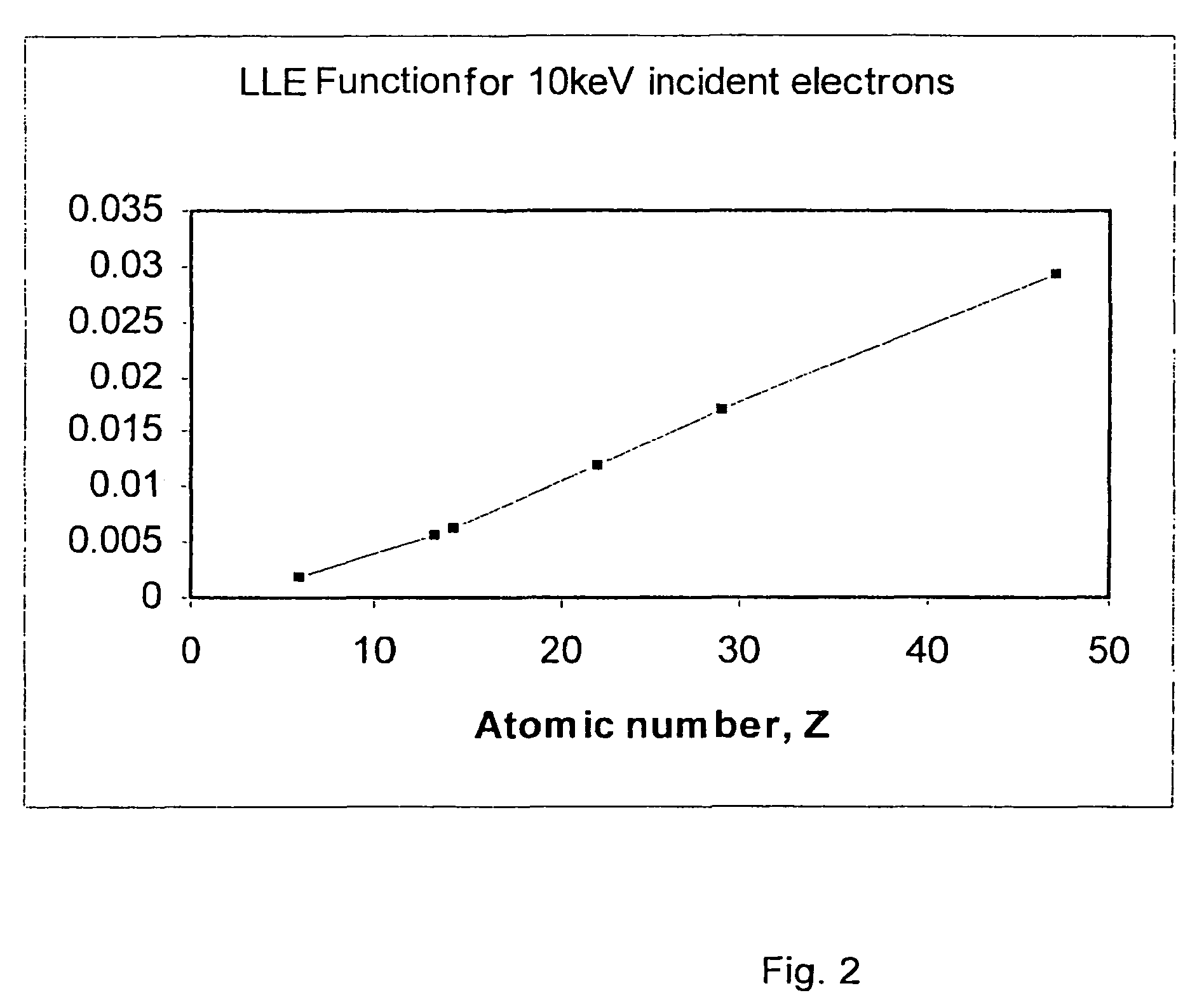
[0063]This first example describes a method of combining LLE and x-ray data to identify the material of an object that is smaller than the x-ray excitation volume (the second region). FIGS. 4a, 4b and 4c show a cross section through a specimen to illustrate electron trajectories that produce the LLE and x-ray signals. The smaller the electron energy loss, the smaller the information volume for the LLE signal (the first region). For example, for an energy loss of 100 eV or less, the information volume is typically of the order of 10 nm across. If there is a small object embedded in the surface and bigger than 10 nm across, the LLE signal would be representative of the material constituting this small object. This is shown in FIG. 4a where it should be noted that the focussed electron beam diameter is less than 10 nm. However, x-rays are emitted all along the electron trajectories (within the second region) so the x-ray spectrum is representative of material from both the small object...

example 2

[0074]This second example describes the use of the invention in combination with a raster scan. If the incident beam is scanned over a raster covering a field of view, the LLE signal can be measured at each point in the raster and converted to an effective Z value. If this effective Z is plotted as a function of beam position, this will provide an image of the material in the field of view showing high resolution material contrast. If the same field of view is scanned while measuring the x-ray spectrum at each point, lower spatial resolution analytical information is obtained. U.S. Pat. No. 5,357,110 describes a method of combining the lower spatial resolution x-ray analytical information with an auxiliary signal such as a backscattered electron signal, to provide a composite image that shows analytical information of element content at the higher spatial resolution of the auxiliary signal.

[0075]We have realised that the same method can be used to combine the very high spatial resol...

example 3

[0076]This third example explains the use of the invention to obtain information upon layered structures.

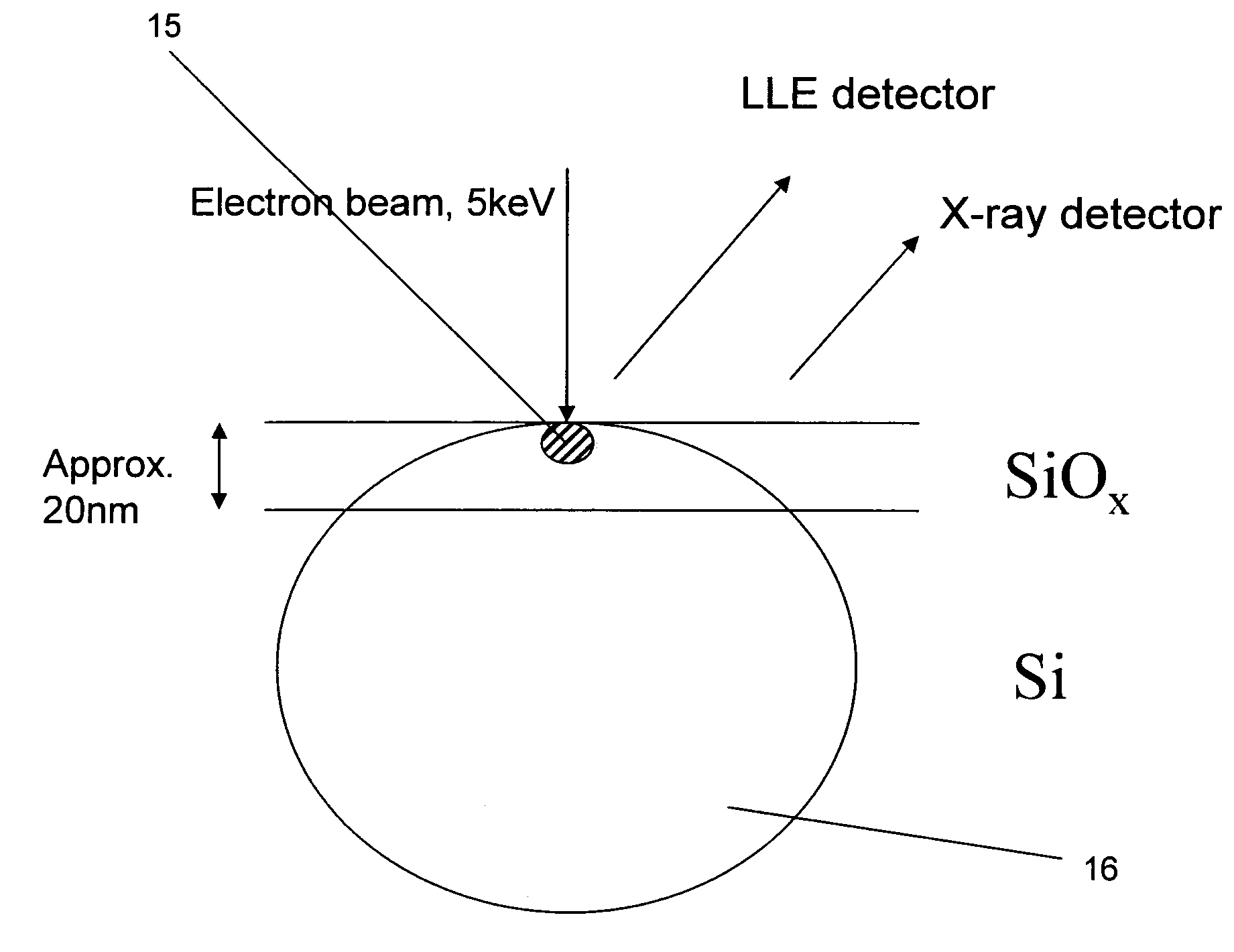
[0077]In this case the specimen consists of a number of layers of unknown composition and thickness. A vertical section can be prepared by focussed ion beam etching (FIB) in an SEM. The etched surface is presented normal to the incident electron beam (a 10 keV beam in this case). FIG. 6 shows a cross section illustrating the electron trajectories through such a specimen. In FIG. 6 the actual compositions of and thicknesses of the layers are shown, these being nickel (100 nm), aluminium (200 nm) and gold (50 nm), these all being sandwiched by a thick layer of silicon upon either side of the three layers.

[0078]When the focussed incident beam is within the Au layer, the LLE signal is generated by a small volume less than the layer thickness and is therefore representative of Au alone. However, the 10 keV incident electrons scatter within the specimen and excite x-rays from the neigh...


PUM

PropertyMeasurementUnit
energyaaaaaaaaaa
energyaaaaaaaaaa
depthaaaaaaaaaa

Abstract

A method and apparatus for quantitative analysis of a material in which an electron beam is caused to impinge upon the material are described. The method comprises detecting low loss electrons (LLEs) received from a first region of the material due to interaction with the electron beam and generating corresponding LLE data. The method further comprises detecting x-rays received from a second region of the material due to interaction with the electron beam and generating corresponding x-ray data, wherein the first and second regions overlap, and analysing the LLE data together with the x-ray data so as to generate compositional data representative of the composition of the first region.

Description

FIELD OF THE INVENTION[0001]The present invention relates to a method of quantitative analysis of a material, in particular using an electron beam technique. A corresponding apparatus is also provided. The invention finds particular application in scanning electronic microscopes (SEM) and provides a means to achieve a high spatial resolution analysis of the specimen by combining information from x-rays and electrons.BACKGROUND TO THE INVENTION[0002]Scanning electron microscopes (SEMs) are common tools for the observation of small features. In this technique, a finely focused electron beam (“probe”) with an energy typically between about 1 keV and 20 keV is scanned across the surface of a sample. At each probe position on the surface, signals are conventionally measured by a number of different types of detector. Commonly, scattered electrons and x-rays are detected and for each signal, magnified images of the specimen are constructed where the signal strength modulates the intensity...

Claims


Application Information

Patent Timeline
Patent Type & Authority Patents(United States)
IPC IPC(8): G01N23/00
CPCG01N23/2252H01J37/244H01J37/256H01J37/28H01J2237/2807H01J2237/24495H01J2237/2804
Inventor STATHAM, PETER JOHNBARKSHIRE, IAN RICHARD
Owner OXFORD INSTR NANOTECH TOOLS
Why Eureka
Try Eureka