Semiconductor memory device adopting improved local input/output line precharging scheme

a memory device and micro-conductor technology, applied in the direction of information storage, static storage, digital storage, etc., can solve the problems of low efficiency in sensing data from memory cells, loss of data quality, so as to reduce voltage, minimize or reduce the disturbance of bit lines, the effect of reducing the disturban

Active Publication Date: 2012-07-17
SAMSUNG ELECTRONICS CO LTD
View PDF15 Cites 384 Cited by
  • Summary
  • Abstract
  • Description
  • Claims
  • Application Information

AI Technical Summary

Benefits of technology

[0013]Example embodiments provide a semiconductor memory device capable of performing a precharging operation on local input / output lines both under a short tRCD condition and under a long tRCD condition. The semiconductor memory device may include a read data path circuit to perform a read operation at a lower voltage at a higher speed and to reduce or minimize bit line disturbance.
[0014]Example embodiments provide a local input / output line precharging scheme for a high-speed semiconductor memory device, which makes it possible to perform a read operation with a lower-voltage at a higher speed and to reduce or minimize bit line disturbance.
[0016]Example embodiments provide a DRAM capable of flexibly controlling a design margin for local input / output line sense amplifiers.
[0028]According to example embodiments, bit line disturbance may be minimized or reduced and a read operation is performed at a lower voltage and at a higher speed. Moreover, the NMOS precharging may be performed under the short tRCD condition and the PMOS precharging is performed under the long tRCD condition. Therefore, the example embodiments may be robust against bit line disturbance and are advantageous for a low-voltage high-speed operation.

Problems solved by technology

For example, when a pair of local input / output lines are maximally amplified to have the operation voltage and a ground voltage, and are precharged to a first voltage, the precharging of the pair of local input / output lines may cause noise to change the level of the first voltage.
In other words, the noise may influence a circuit which generates the first voltage, resulting in a drop in efficiency in sensing data from memory cells.
A general precharging circuit to precharge a pair of local input / output lines in an active mode may not exhibit a satisfactory operation quality both under a short / RAS to / CAS delay time (hereinafter, referred to as a tRCD) condition and under a long tRCD condition.
If the precharging circuit does not exhibit a satisfactory operation quality under the short tRCD condition, a bit line disturbance phenomenon may occur, and if the precharging circuit does not exhibit a satisfactory operation quality under the long tRCD condition, a low-voltage high-speed operation quality may be degraded.

Method used


Image

  • Semiconductor memory device adopting improved local input/output line precharging scheme
  • Semiconductor memory device adopting improved local input/output line precharging scheme
  • Semiconductor memory device adopting improved local input/output line precharging scheme

Examples


Embodiment Construction

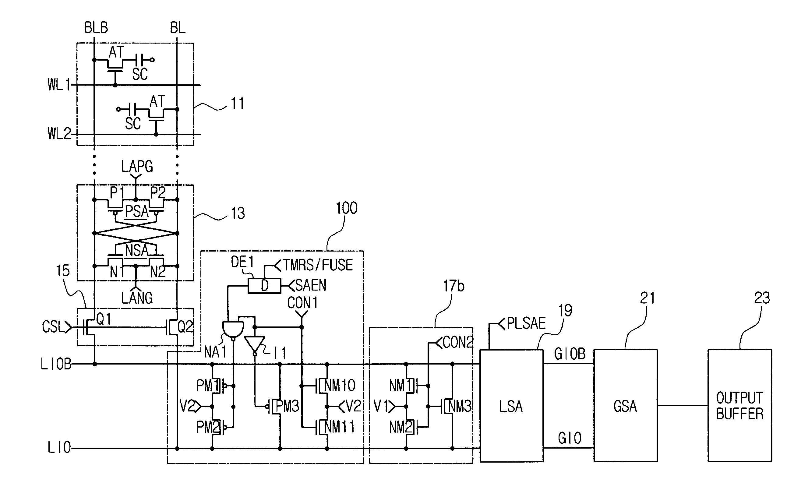
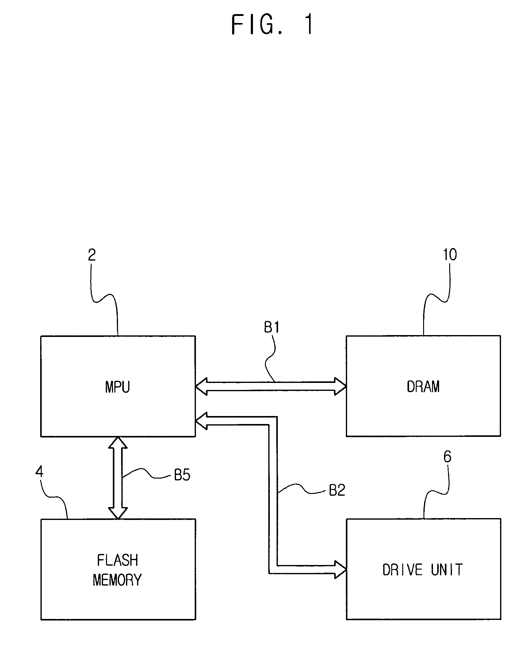
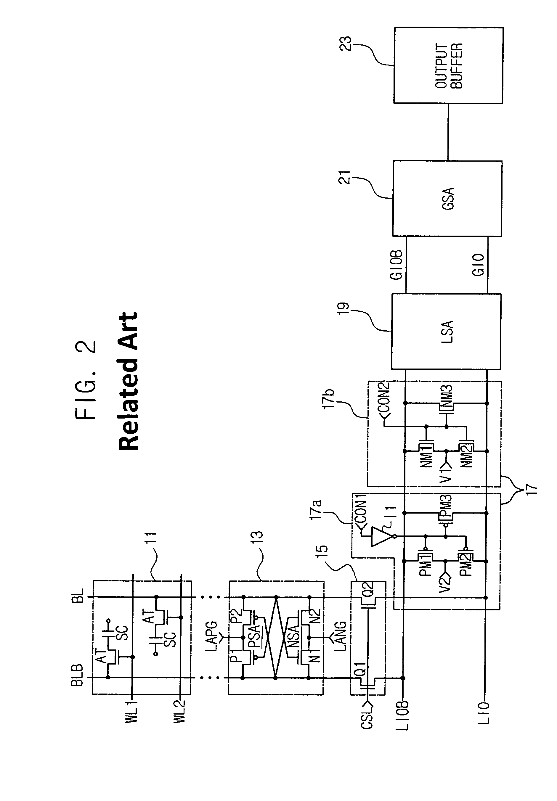
[0040]Example embodiments will now be described more fully with reference to the accompanying drawings. In the drawings, the thicknesses of layers and regions may be exaggerated for clarity.

[0041]Specific structural and functional details disclosed herein are merely representative for purposes of describing example embodiments. Example embodiments may, however, may be embodied in many alternate forms and should not be construed as limited to only the embodiments set forth herein.

[0042]Accordingly, while example embodiments are capable of various modifications and alternative forms, embodiments thereof are shown by way of example in the drawings and will herein be described in detail. It should be understood, however, that there is no intent to limit example embodiments to the particular forms disclosed, but on the contrary, example embodiments are to cover all modifications, equivalents, and alternatives falling within the scope of example embodiments. Like numbers refer to like ele...


PUM


Abstract

A semiconductor memory device capable of preventing or minimizing bit line disturbance and performing a low-voltage high-speed operation includes a read data path circuit including a bit line sense amplifier, a local input / output line sense amplifier, a column selecting unit to operationally connect bit lines connected to the bit line sense amplifier to local input / output lines connected to the local input / output line sense amplifier in response to a column selection signal, and a local input / output line precharging unit to precharge the pair of local input / output lines by a first precharging unit, equalizing the pair of local input / output lines by an equalizing unit, and to precharge the local input / output lines by a second precharging unit following an elapsed time after the bit line sense amplifier is activated, while the column selection is deactivated.

Description

PRIORITY STATEMENT[0001]This U.S. non-provisional patent application claims Priority Under 356 U.S.C. §119 to Korean Patent Application 10-2008-0129775, filed on Dec. 19, 2008, in the Korean Intellectual Property Office (KIPO), the entire contents of which are incorporated herein by reference.BACKGROUND[0002]1. Field[0003]Example embodiments of the present invention relate to a semiconductor memory device, and in particular, to a read data path circuit for use in a semiconductor integrated circuit device such as a dynamic random access memory.[0004]2. Description of the Related Art[0005]There is a movement towards developing semiconductor memory devices including dynamic random access memories (hereinafter, referred to as DRAMs) with a high degree of integration and high speed. DRAMs have memory cells and are generally adopted as main memories for electronic systems. Each of the memory cells includes one access transistor and one storage capacitor[0006]Referring to FIG. 1, in a gene...

Claims


Application Information

Patent Timeline
Patent Type & Authority Patents(United States)
IPC IPC(8): G11C7/12
CPCG11C5/025G11C7/1048G11C7/1051G11C7/1069G11C11/4096G11C11/4097G11C2207/002G11C11/4093G11C11/4074G11C11/4091
Inventor SEO, SEONG-YOUNG
Owner SAMSUNG ELECTRONICS CO LTD
Why Eureka
Try Eureka