Nonvolatile semiconductor memory device

a semiconductor and storage device technology, applied in semiconductor devices, electrical equipment, instruments, etc., can solve the problem of high write voltage of conventional nonvolatile memory, and achieve the effect of improving the charge retention characteristics of floating gates, excellent characteristics, and manufacturing without loss of productivity

Active Publication Date: 2012-07-24
SEMICON ENERGY LAB CO LTD
View PDF66 Cites 0 Cited by
  • Summary
  • Abstract
  • Description
  • Claims
  • Application Information

AI Technical Summary

Benefits of technology

[0009]A gate insulating layer provided between the floating gate and the semiconductor layer is required to be thin in thickness so that charges can be injected into the floating gate at a low voltage. On the other hand, in order to stably retain the charges of the floating gate for a long period of time, the film thickness is required to be thick thereby preventing leakage of the charges.
[0010]Eventually, a conventional nonvolatile memory requires high write voltage. Besides, error detection and error correction are carried out by providing a redundant memory cell or devising a controller to counter degradation of charge retention characteristics by repetitive rewriting, thereby insuring reliability.
[0011]In view of the above, it is an object of the present invention to provide a nonvolatile semiconductor memory device excellent in writing characteristics and charge retention characteristics.
[0018]In the case of forming a floating gate over a semiconductor layer with a first insulating layer serving as a tunnel insulating layer therebetween, the floating gate is formed of a semiconductor material at least containing germanium, whereby charges can be easily injected from the semiconductor layer to the floating gate and charge retention characteristics of the floating gate can be improved.
[0019]Further, when the floating gate is formed using a material having similar properties to silicon, a nonvolatile semiconductor memory device with excellent characteristics can be manufacture without loss of the productivity. Since germanium is a semiconductor and is a material of the group XIV of the periodic table of elements as the same as silicon, a thin film can be microfabricated without putting a load on manufacturing facilities.

Problems solved by technology

Eventually, a conventional nonvolatile memory requires high write voltage.

Method used


Image

  • Nonvolatile semiconductor memory device
  • Nonvolatile semiconductor memory device
  • Nonvolatile semiconductor memory device

Examples


embodiment 1

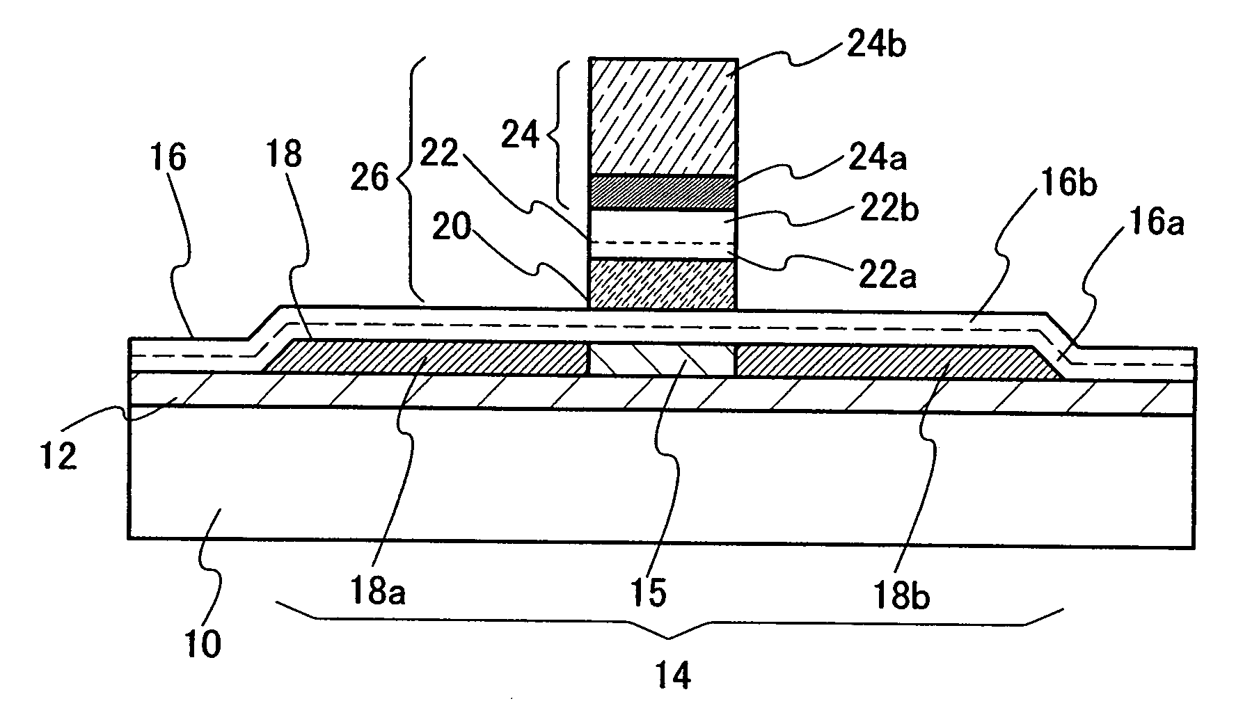
[0128]This embodiment will describe one example of a nonvolatile semiconductor memory device with reference to drawings. A description will be given below of the case where a nonvolatile memory element for forming a memory section is formed at the same time as an elements such as a transistor for forming a logic portion that is provided over the same substrate as the memory section and performs control of the memory section or the like in a nonvolatile semiconductor memory device.

[0129]First, an equivalent circuit of a memory section in the nonvolatile semiconductor memory device is shown in FIG. 8.

[0130]In the memory section described in this embodiment, a plurality of memory cells each including a selecting transistor and a nonvolatile memory element is provided. In FIG. 8, one memory cell includes a selecting transistor S01 and a nonvolatile memory element M01. Similarly, each memory cell includes a selecting transistor S02 and a nonvolatile memory element M02, a selecting transi...

embodiment 2

[0177]This embodiment will explain the case where a plurality of nonvolatile memory elements are provided on one island-shaped semiconductor layer in the structure shown in Embodiment 1, with reference to the drawings. It is to be noted that the same portions as those in the above embodiment are denoted by the same reference numerals, and explanation thereof will be omitted. FIG. 37 shows a top-view, and FIGS. 38A and 38B show cross-sectional views taken along line E-F and line G-H in FIG. 37.

[0178]The nonvolatile semiconductor memory device described in this embodiment includes island-shaped semiconductor layers 200a and 200b electrically connected to bit lines BL0 and BL1, respectively. Each of the island-shaped semiconductor layers 200a and 200b is provided with a plurality of nonvolatile memory elements (see FIGS. 37, and 38A and 38B). Specifically, over the semiconductor layer 200a, a NAND cell 202a including a plurality of nonvolatile memory elements M0 to M31 is provided betw...

embodiment 3

[0182]This embodiment will explain a manufacturing method of a nonvolatile semiconductor memory device which is different from one in Embodiment 1 with reference to the drawings. It is to be noted that the same portions as those in the above embodiment are denoted by the same reference numerals, and explanation thereof will be omitted. In FIGS. 22A to 24B, portions along line A-B and line C-D each includes a thin film transistor provided in a logic section, a portion along line E-F includes a nonvolatile memory element provided in a memory section, and a portion along line G-H includes a thin film transistor provided in the memory section.

[0183]First, the structure shown in FIG. 18C is prepared in the like manner. Thereafter, the resist 122 is removed, and a second insulating layer 128 is formed so as to cover semiconductor layers 104, 106, and 110, and a first insulating layer 116 and a charge accumulation layer 121 functioning as a floating gate formed over a semiconductor layer 1...


PUM


Abstract

A semiconductor layer having a channel formation region provided between a pair of impurity regions spaced from each other is provided, and a first insulating layer a floating gate, a second insulating layer, and a control gate are provided above the semiconductor layer. The semiconductor material forming the floating gate preferably has a band gap smaller than that of the semiconductor layer. The band gap of a channel formation region in the semiconductor material forming the floating gate is preferably smaller than that of the semiconductor layer by 0.1 eV or more.

Description

BACKGROUND OF THE INVENTION[0001]1. Field of the Invention[0002]The present invention relates to a nonvolatile semiconductor storage device that is electrically writable, readable, and erasable, and its manufacturing method. In particular, the present invention relates to a structure of a floating gate in the nonvolatile semiconductor storage device.[0003]2. Description of the Related Art[0004]The market in nonvolatile memories in which data can be electrically rewritten and data can be stored even after the power is turned off is expanding. Features of a nonvolatile memory lie in that its structure is similar to that of a MOSFET (Metal Oxide Semiconductor Field Effect Transistor) and a region capable of accumulating charges for a long period of time is provided over a channel formation region. The charge storage region is formed over an insulating layer and is electrically isolated from the surroundings; therefore, it is also referred to as a floating gate. A floating gate is surro...

Claims


Application Information

Patent Timeline
Patent Type & Authority Patents(United States)
IPC IPC(8): H01L29/76
CPCH01L21/28273H01L21/84H01L27/105H01L27/115H01L27/11519H01L27/11521H01L27/11524H01L27/11526H01L27/11546H01L27/1203H01L29/42324H01L29/66825H01L29/7881G11C16/349H01L27/1214H01L29/78696H01L29/40114H01L27/1237H10B69/00H10B41/10H10B41/30H10B41/35H10B41/40H10B41/49
Inventor YAMAZAKI, SHUNPEIASAMI, YOSHINOBUTAKANO, TAMAEFURUNO, MAKOTO
Owner SEMICON ENERGY LAB CO LTD
Why Eureka
Try Eureka