

Fabrication of low defectivity electrochromic devices
a technology of electrochromic devices and low defectivity, which is applied in the direction of manufacturing tools, solid-state diffusion coatings, instruments, etc., can solve the problems of high defectivity of prior electrochromic devices, impaired electrochromic transition, and defect manifesting, etc., and achieve high defectivity.
- Summary
- Abstract
- Description
- Claims
- Application Information
AI Technical Summary
Benefits of technology
Problems solved by technology
Method used
Image

Examples
Embodiment Construction
[0028]Electrochromic Devices
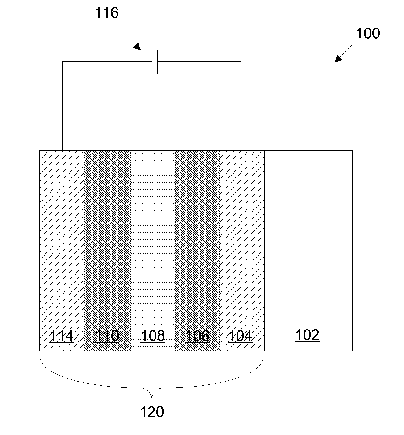
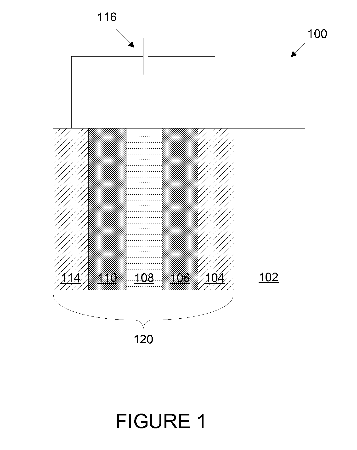
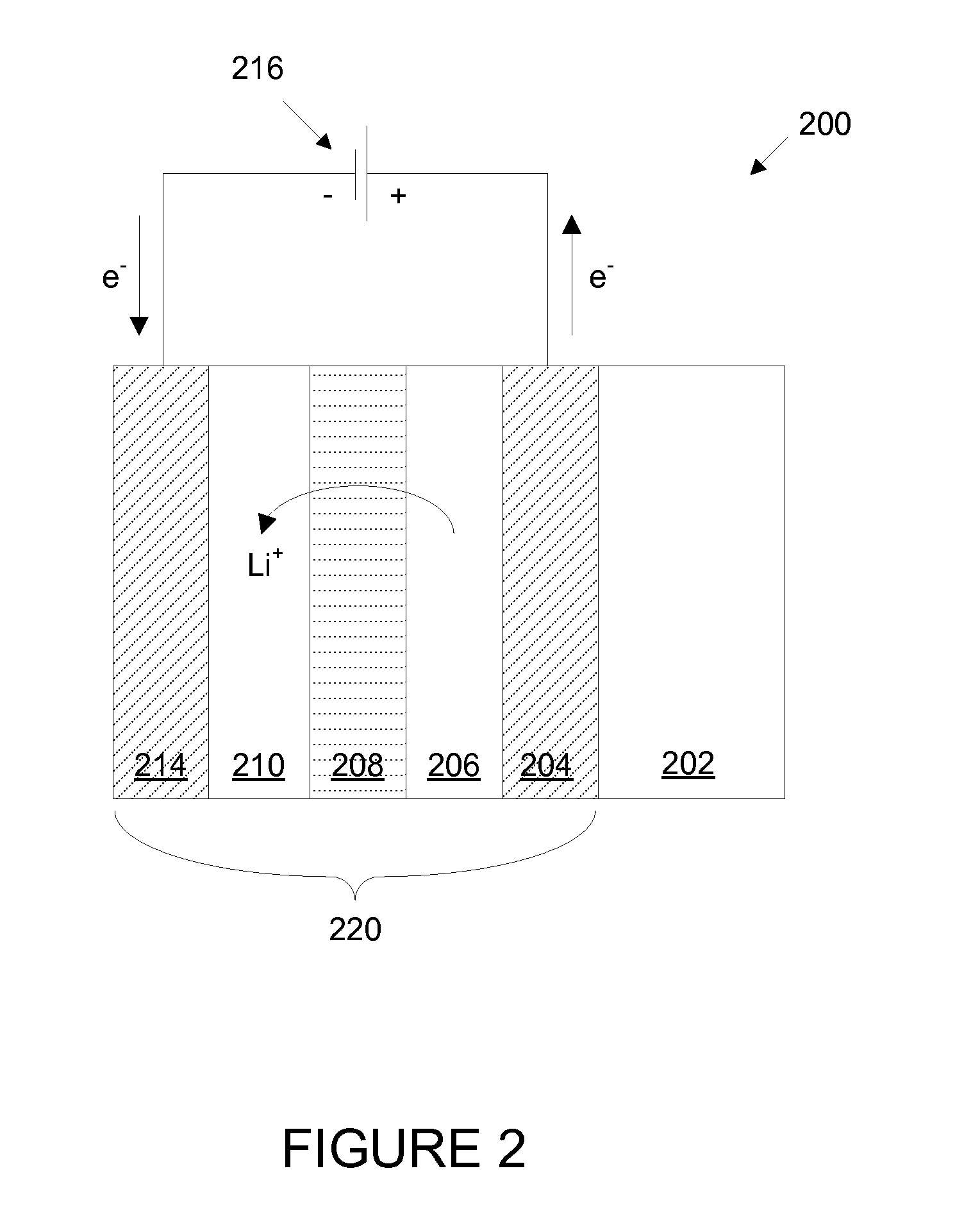
[0029]A schematic cross-section of an electrochromic device 100 in accordance with some embodiments is shown in FIG. 1. The electrochromic device includes a substrate 102, a conductive layer (CL) 104, an electrochromic layer (EC) 106, an ion conducting layer (IC) 108, a counter electrode layer (CE) 110, and a conductive layer (CL) 114. Elements 104, 106, 108, 110, and 114 are collectively referred to as an electrochromic stack 120. A voltage source 116 operable to apply an electric potential across the electrochromic stack 120 effects the transition of the electrochromic device from, e.g., a bleached state to a colored state. In other embodiments, the order of layers is reversed with respect to the substrate. That is, the layers are in the following order: substrate, conductive layer, counter electrode layer, ion conducting layer, electrochromic material layer, conductive layer.
[0030]It should be understood that the reference to a transition between a ble...
PUM
| Property | Measurement | Unit |
|---|---|---|
| size | aaaaa | aaaaa |
| size | aaaaa | aaaaa |
| surface roughness | aaaaa | aaaaa |
Abstract
Description
Claims
Application Information