Active matrix substrate and display device having the same

a technology of active matrix substrate and display device, which is applied in the direction of static indicating device, television system, instruments, etc., can solve the problems of difference in pixel capacitance of charged amount, and achieve the effect of suppressing the deterioration of display quality, improving moving image display performance, and short tim

Active Publication Date: 2012-09-04
SHARP KK
View PDF60 Cites 2 Cited by
  • Summary
  • Abstract
  • Description
  • Claims
  • Application Information

AI Technical Summary

Benefits of technology

[0083]According to the fourth aspect of the present invention, since the control signal line for the charge sharing is disposed along each of the scanning signal lines and the switching element for the charge sharing is provided corresponding to each of the control signal lines for each of the data signal lines, there exist the switching elements for each of the data signal lines in numbers equal to the number of the scanning signal lines and the charge transfer is performed by these switching elements between the data signal lines for the charge sharing period. Thereby, it is possible to cause the potential in the data signal line to reach the intermediate potential uniformly in the entire active matrix substrate, even when the charge sharing period is shorter or a larger active matrix substrate is employed. Further, since there exist the switching element for the charge sharing at each pixel and the control signal line for turning on and off the switching element in each pixel line, the arrangement of the switching elements and the control signal lines for the charge sharing matches the pixel arrangement of image to be formed on the active matrix substrate and the regularity of the pixel arrangement is not disturbed by the addition of the switching elements and the control signal lines for the charge sharing.
[0084]According to the fifth aspect of the present invention, the charge transfer is performed between the data signal lines for the charge sharing period by the switching element group disposed in the neighborhood of one end of the data signal lines and the switching element group disposed in the neighborhood of the other end of the data signal lines. Accordingly, the potential in the data signal line can be made uniform immediately after the charge sharing period within the active matrix substrate, compared to a conventional charge sharing method in which the charge transfer between the data signal lines is performed by a switching circuit in the data signal line drive circuit.
[0085]According to the sixth aspect of the present invention, the charge transfer is performed for the charge sharing period between the data signal lines via the switching element which is turned on and off by the non-display area control signal line in the non-display area. Thereby it is possible to accelerate the charge transfer between the data signal lines in the charge sharing period while suppressing the deterioration of an aperture ratio.
[0086]According to the seventh aspect of the present invention, since the pixel electrode is disposed so as to overlap with the charge sharing control signal line, it is possible to secure a larger area for the pixel portion and thereby to increase the aperture ratio.
[0087]According to the eighth aspect of the present invention, since the electrode portion (connection electrode portion) connecting the charge sharing switching element to the data signal line is disposed so as not to overlap with the charge sharing control signal line, it is possible to repair a short-circuit fault by cutting the connection electrode portion with laser irradiation or the like, when a transistor serving as the switching element for the charge sharing is short-circuited and always in a conduction state caused by a defect such as a film residual in a channel portion of the transistor (case of a transistor short-circuit fault). Further, such a disposition configuration is effective to reduce a probability of causing a short-circuit between the charge sharing control signal line and the data signal line.
[0088]According to the ninth aspect of the present invention, the lengths of the interconnections for connecting the charge sharing switching element and the two neighboring data signal lines to be short-circuited, when the charge sharing switching element is turned on, are the same as each other, and thereby it is possible to transfer the charge in the charge sharing period symmetrically between the neighboring data signal lines.
[0089]According to the tenth aspect of the present invention, in the active matrix type display device employing the charge sharing method, each of the data signal lines is short-circuited with another data signal line neighboring thereto for the charge sharing period when the polarity of the data signal is inverted, and thereby the charge is transferred between the neighboring data signal lines to reduce power consumption. Further, the difference occurs in the charged amount of the pixel capacitance between the two lines of the polarity inversion unit and the horizontal line irregularity is viewed sometimes in the liquid crystal display device using the conventional 2H dot inversion drive method, for example. However, in this display device, the charge sharing period, when each of the data signal lines is short-circuited with another data signal line neighboring thereto, is provided for each horizontal period and such charged amount difference or horizontal line irregularity are suppressed. Further, since each of the data signal lines is connected with another data signal line neighboring thereto via the plurality of charge sharing switching elements, the charge transfer is performed in a short time between the data signal lines in the charge sharing period. As a result, it is possible to suppress the deterioration of display quality caused by the difference in the charged amount or the shortage of charging in the pixel capacitance, even when a larger size or a higher resolution is employed in the display device and the drive frequency thereof is increased.
[0090]According to the eleventh aspect of the present invention, the period of the polarity inversion in the data signal corresponds to two or more horizontal periods and it is possible to reduce a heat value and power consumption in the data signal line drive circuit. Generally, as the polarity inversion period becomes longer, that is, “n” becomes larger in the “nH” dot inversion drive method to be employed, the heat value and the power consumption are reduced more in the data signal line drive circuit. Further, for the same reason as in the tenth aspect of the present invention, it is possible to suppress the deterioration of display quality caused by the difference in the charged amount or the shortage of charging in the pixel capacitance, even when a larger size or a higher resolution is employed in the display device and the drive frequency thereof is increased.
[0091]According to the twelfth aspect of the present invention, the data signal lines on the active matrix substrate are short-circuited with each other for the charge sharing period (a predetermined period for every one horizontal period) also by the switch circuit within the data signal line drive circuit, and thereby the charge transfer is further accelerated between the data signal lines.
[0092]According to the thirteenth aspect of the present invention, since a fixed voltage is applied to the data signal lines when the data signal lines on the active matrix substrate are short-circuited with each other by the switch circuit within the data signal line drive circuit (charge sharing period), the voltage of each of the data signal lines immediately after the charge sharing period always becomes the same voltage, even when a correction amount of the data signal for compensating gradation dependence of a pull-in voltage due to a parasitic capacitance of each pixel formation portion is different depending on gradation to be displayed. Thereby, it is possible to suppress the horizontal line irregularity to occur, even when the data signal is corrected according to the gradation to be displayed.
[0093]According to the fourteenth aspect of the present invention, the potential of each of the data signal lines becomes to have the middle value between the minimum value and the maximum value of the data signal immediately after the charge sharing period, and thereby it is possible to make uniform the charged amount of the pixel capacitance without depending on the polarity of the data signal to be applied to the pixel electrode.
[0094]According to the fifteenth aspect of the present invention, since the plurality of data signals applied to the plurality of data signal lines, respectively, on the active matrix substrate are voltage signals which invert the polarities every predetermined number of data signal lines, the voltage of each of the data signal lines becomes approximately the same as a DC level of the data signal in the charge sharing period when each of the plurality of data signal lines is short-circuited with another data signal line neighboring thereto. This means that the voltage of each of the data signal lines becomes to have a value corresponding to a black display (black voltage). Meanwhile, each of the scanning signal lines is in the selected state for the charge sharing period at least once after the predetermined pixel value holding period has elapsed from the time the scanning signal line was selected in the effective scanning period for writing a pixel value. Thereby, since a period until the scanning signal line goes into the selected state next in the effective scanning period for writing the pixel value becomes available for a period of the black display, it is possible to insert a black with the same length into all the display lines and to improve the display performance for a moving image by realizing an impulse type drive securing a sufficient black insertion period without shortening the charging time of the pixel capacitance for writing the pixel value. Further, it is not necessary to increase an operation speed of the data signal line drive circuit or the like for inserting the black.
[0095]According to the sixteenth aspect of the present invention, the scanning signal line which was in the selected state for the effective scanning period is in the selected state for the charge sharing period the plurality of times after the pixel value holding period has elapsed from the time when the selected state changed to the unselected state and before the scanning signal line goes to the selected state during the effective scanning period in the next frame period. Thereby, it is possible to cause display luminance to be at a sufficient black level in the black display period for the impulse type drive.
[0092]According to the thirteenth aspect of the present invention, since a fixed voltage is applied to the data signal lines when the data signal lines on the active matrix substrate are short-circuited with each other by the switch circuit within the data signal line drive circuit (charge sharing period), the voltage of each of the data signal lines immediately after the charge sharing period always becomes the same voltage, even when a correction amount of the data signal for compensating gradation dependence of a pull-in voltage due to a parasitic capacitance of each pixel formation portion is different depending on gradation to be displayed. Thereby, it is possible to suppress the horizontal line irregularity to occur, even when the data signal is corrected according to the gradation to be displayed.
[0097]According to the eighteenth aspect of the present invention, the buffers within the data signal line drive circuit are halted for the charge sharing period when each of the data signal lines is short-circuited with another data signal line neighboring thereto, and thereby it is possible to reduce power consumption of the data signal line drive circuit.

Problems solved by technology

Therefore, the drive of the first line requires a longer time for charging the data signal line compared to the drive of the second line, and resultantly a difference of charged amount in the pixel capacitance is caused between the first line and the second line.

Method used


Image

  • Active matrix substrate and display device having the same
  • Active matrix substrate and display device having the same
  • Active matrix substrate and display device having the same

Examples


first embodiment

1. First Embodiment

1.1 Configuration and Operation

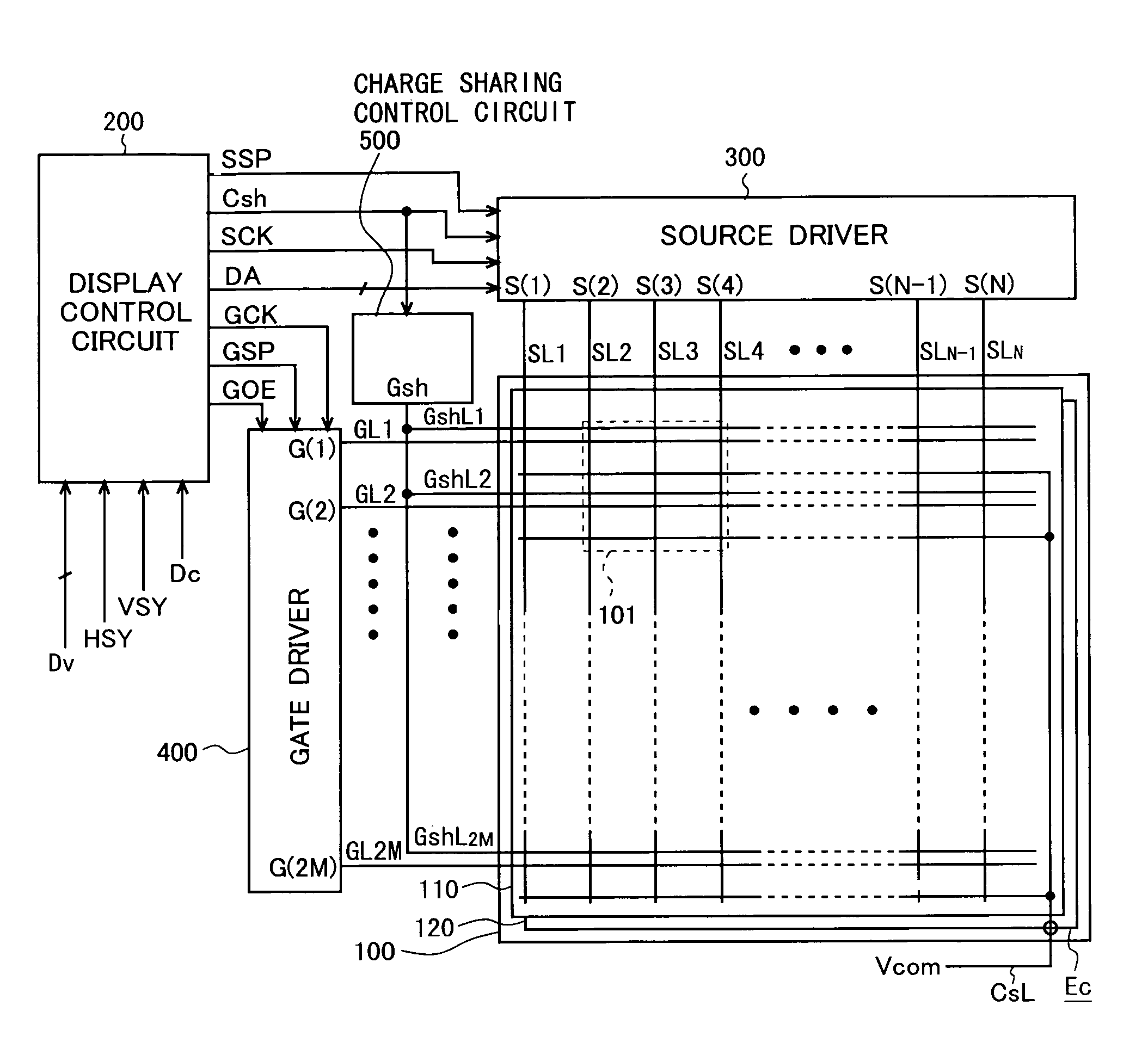
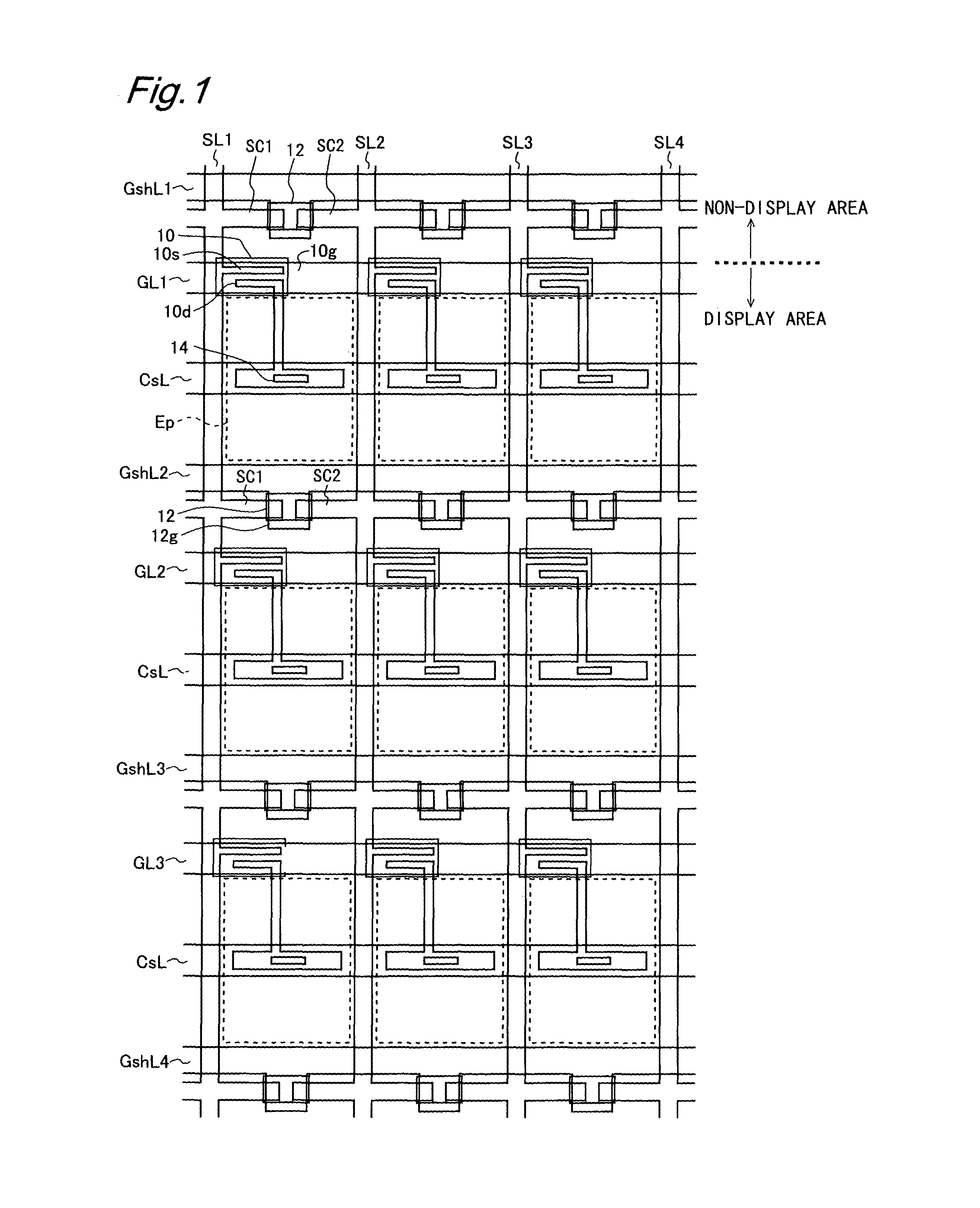
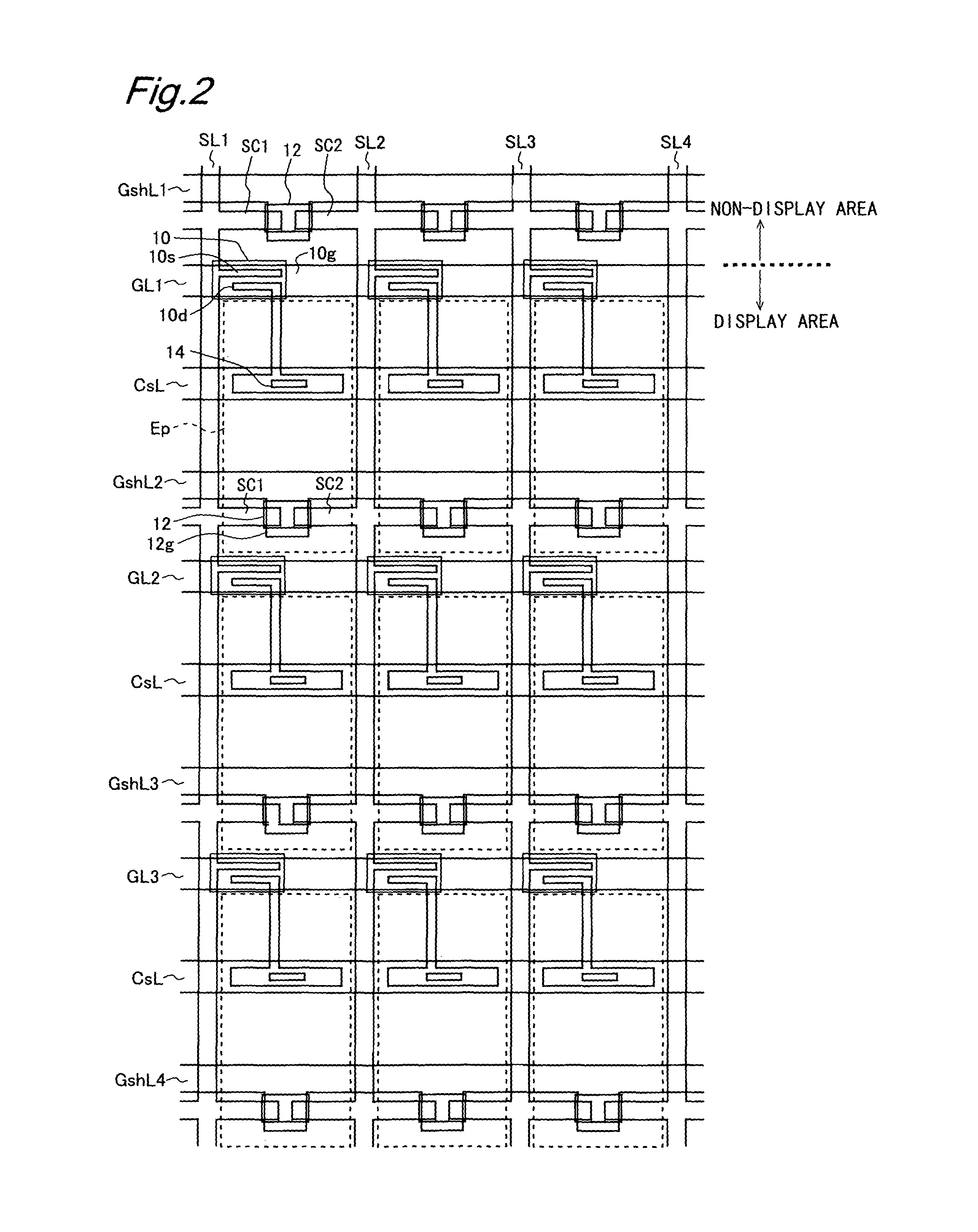
[0159]A first embodiment will be described for an example of a liquid crystal display device using an active matrix substrate according to the present invention. FIG. 4 is a block diagram showing a configuration of the liquid crystal display device according to the present embodiment. FIG. 5 is a circuit diagram showing an equivalent circuit of the active matrix substrate 110 according to the present embodiment, and shows an electrical configuration of a part (part corresponding to neighboring four pixels) 101 of the active matrix substrate 110.

[0160]This liquid crystal display device includes: a source driver 300 as a data signal line drive circuit; a gate driver 400 as a scanning signal line drive circuit; a charge sharing control circuit 500; an active matrix type display part 100 using the active matrix substrate 110; and a display control circuit 200 for controlling the source driver 300, gate driver 400, and charge sharing cont...

second embodiment

2. Second Embodiment

[0190]An entire configuration of a liquid crystal display device according to the present embodiment is the same as that of the liquid crystal display device according to the first embodiment as shown in FIG. 4, and a part as same as or corresponding to that in the first embodiment is denoted by the same reference symbol and detailed description will be omitted. In the present embodiment, an internal configuration of the source driver is different from that of a source driver 300 in the first embodiment. Accordingly, the configuration of the source driver will be described below.

[0191]The source driver in the present embodiment is also composed of the data signal generation part 302 and the output part 304 as in the first embodiment shown in FIG. 6, but the internal configuration of the output part 304 is different from that in the first embodiment. The internal configuration and operation of the data signal generation part 302 is the same as those in the convent...

third embodiment

3. Third Embodiment

[0199]The present invention can be applied to a liquid crystal display device employing a drive method in which a upper half part and a lower half part of a display part 100 are driven by different drive circuits (hereinafter, called “upper-and-lower division drive method”). A third embodiment will be described below for such a liquid crystal display device using an active matrix substrate according to the present invention.

[0200]FIG. 15 is a block diagram showing a configuration of a liquid crystal display device according to the present embodiment. In a active matrix substrate 112 of this liquid crystal display device, each source line is composed of a upper source line SLi(upper) and a lower source line SLi(lower) which are electrically separated from each other at center. The other constituents of the active matrix substrate 112 are the same as those of the active matrix substrate 110 in the first embodiment. Accordingly, a pixel circuit configuration of the a...


PUM


Abstract

In at least one embodiment of the present invention, deterioration of display quality is prevented from occurring in a display device provided with an active matrix substrate even when a larger size or a higher resolution is employed and a drive frequency is increased. In an active matrix substrate of a liquid crystal display device, a charge sharing control signal line is disposed so as to be arranged along each gate line and charge sharing TFTs are provided for each source line in numbers equal to the number of the gate lines. The gate terminal of the charge sharing TFT is connected to the charge sharing control signal line and the source and drain terminals are connected with neighboring source lines via connection electrode portions, respectively. Each of the charge sharing control signal lines is provided with a signal which turns on the charge sharing TFT for a predetermined period of every one horizontal period.

Description

TECHNICAL FIELD[0001]The present invention relates to an active matrix substrate using switching elements such as thin film transistors and an active matrix type display device such as a liquid crystal display device having the same.BACKGROUND ART[0002]An active matrix substrate is widely used in an active matrix type display device such as a liquid crystal display device and an EL (Electroluminescence) display device. For example, the main part of the active matrix type liquid crystal display device is composed of a liquid crystal panel and drive circuits thereof, and the liquid crystal panel typically includes: the active matrix substrate having pixel circuits disposed in a matrix, each of which contains a thin film transistors (hereinafter, simply abbreviated as “TFT”) as a switching element and a pixel electrode and the like; an opposite substrate of a transparent insulating substrate such as a glass plate having an opposite electrode and an alignment film sequentially deposited...

Claims


Application Information

Patent Timeline
Patent Type & Authority Patents(United States)
IPC IPC(8): G09G3/36
CPCG02F1/13624G09G3/3648G09G3/3614G09G3/3677G09G3/3688G09G2310/0291G09G2310/061G09G2310/08G09G2320/0252G09G2320/0261G09G2330/023
Inventor TSUBATA, TOSHIHIDE
Owner SHARP KK
Why Eureka
Try Eureka