Substrate processing apparatus and reaction tube for processing substrate

a substrate processing and reaction tube technology, applied in liquid surface applicators, coatings, chemical vapor deposition coatings, etc., can solve the problems of increasing the manufacturing cost of such apparatuses, reducing the cost performance of such apparatuses, and the inability to prevent the thermal degradation of quartz reaction tubes completely. , to achieve the effect of reducing the manufacturing cost of the substrate processing apparatus, low cost and high efficiency

Active Publication Date: 2012-10-23
KOKUSA ELECTRIC CO LTD
View PDF18 Cites 13 Cited by
  • Summary
  • Abstract
  • Description
  • Claims
  • Application Information

AI Technical Summary

Benefits of technology

[0014]Objects of the present invention are to perform a film-forming process at a higher temperature, reduce the manufacturing costs of a substrate processing apparatus, and form a silicon film for a solar battery with low costs or high efficiency.

Problems solved by technology

These requirements increase manufacturing costs of such apparatuses but reduce cost performances of the apparatuses.
However, although a cooling mechanism can be simply installed, it is impossible to prevent thermal degradation of the quartz reaction tube completely, and epitaxial substrate processing apparatuses using such quartz reaction tubes having high pressure resistance are expensive.
However, since such apparatuses use heating sources having short lifespan such as a high frequency generator or a lamp heating source, there arises a problem of low productivity.
Furthermore, in the case of using monosilane (SiH4) source gas that easily undergoes thermal decomposition, since hot-wall type processing is necessary, a cooling mechanism may not be installed, and moreover, silicon generated by decomposition of the monosilane source gas may easily be attached and deposited onto the inner wall of a reaction tube as well as the surface of a wafer.
In the case where a reaction tube is made of quartz, due to the difference between thermal expansion coefficients of a silicon film and the reaction tube, the silicon film may be cracked or stripped to cause, for example, devitrification of the reaction tube, and thus the inner wall of the reaction tube may be seriously damaged and weakened.
Therefore, it has been difficult to use such a reaction tube as a production apparatus due to safety concerns.
In addition, silicon stripped from the inner wall of a reaction tube contaminates substrates.
However, the use of amorphous silicon thin films results in low solar energy conversion efficiency and limited application fields.

Method used


Image

  • Substrate processing apparatus and reaction tube for processing substrate
  • Substrate processing apparatus and reaction tube for processing substrate
  • Substrate processing apparatus and reaction tube for processing substrate

Examples


first embodiment

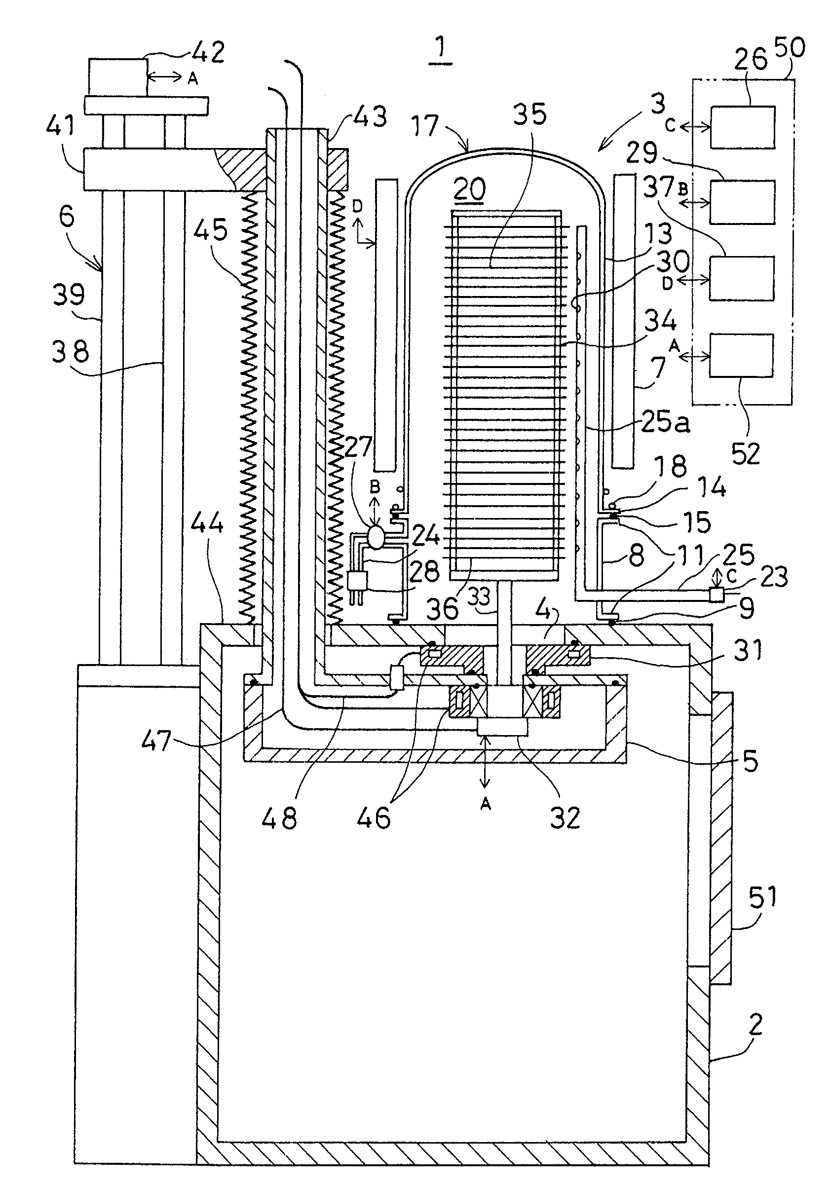
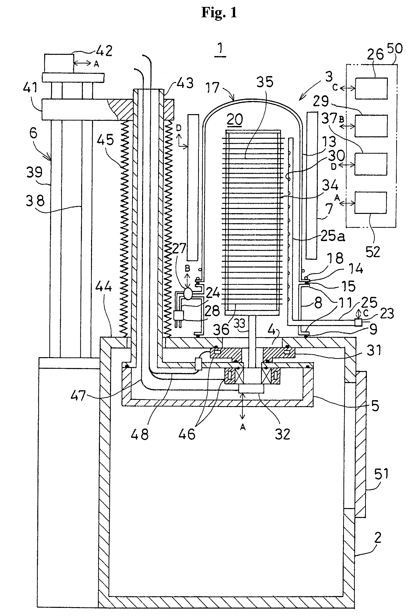
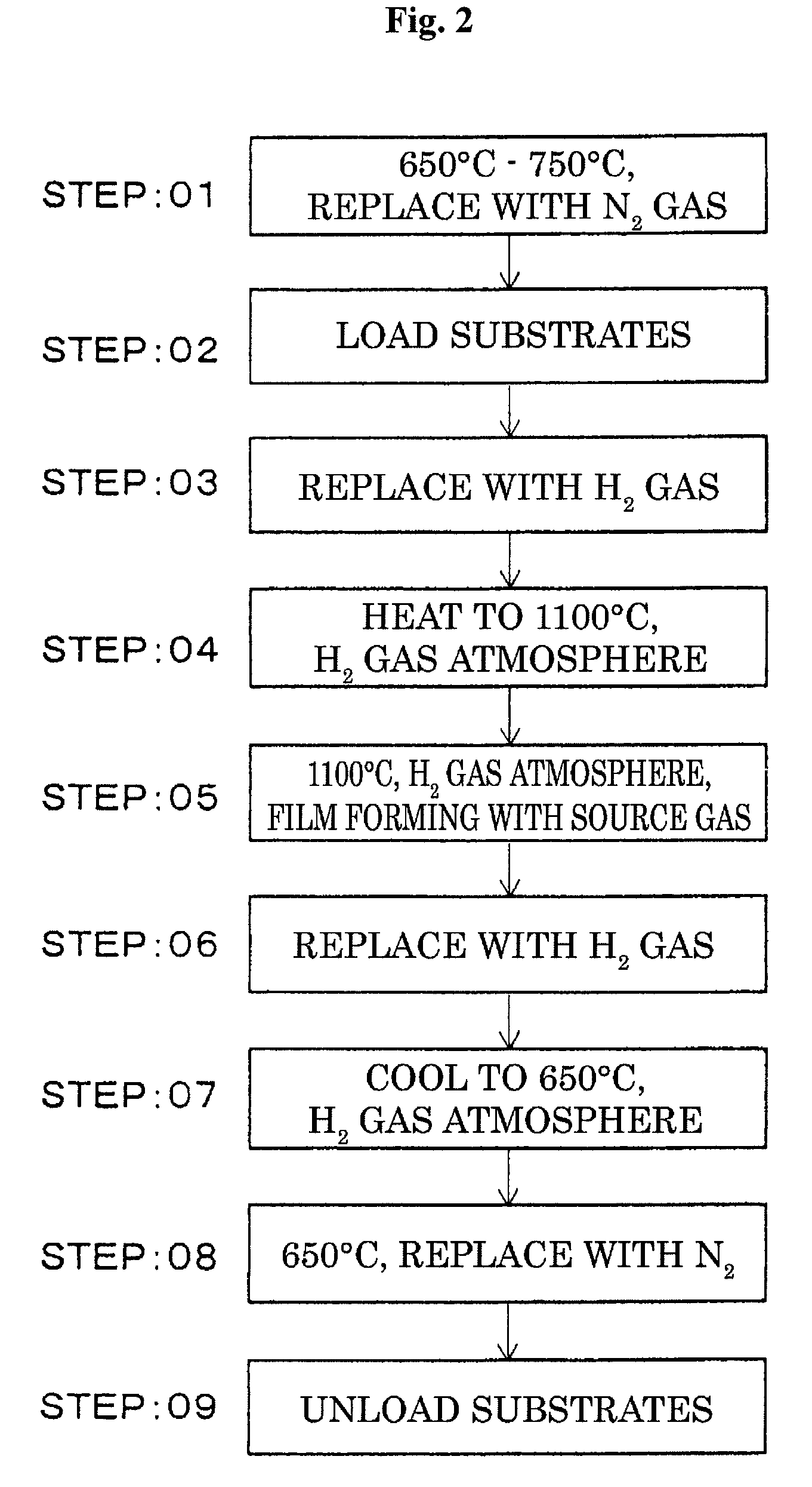
[0029]First, a first embodiment will be described with reference to FIG. 1. In the following description, a batch type substrate processing apparatus including a vertical furnace will be described as an example of a substrate processing apparatus 1, and substrates to be processed are wafers.

[0030]A process furnace 3 is erected on an airtight preliminary chamber 2, and the preliminary chamber 2 communicates with a process furnace 3 through a furnace port 4. An elevator unit 5 is accommodated in the preliminary chamber 2, and the elevator unit 5 is configured to be moved upward and downward by an elevating mechanism such as a boat elevator 6.

[0031]First, the process furnace 3 will be described.

[0032]At the upper side of the preliminary chamber 2, a heater 7 is installed concentrically with the furnace port 4 as a heating mechanism. The heater 7 has a cylindrical shape and is configured by a heater wire and a insulating material disposed around the heater wire. The heater 7 is vertical...

second embodiment

[0089]the present invention will now be described with reference to FIG. 4.

[0090]In the first embodiment of the present invention, the process chamber 17 is constituted by the alloy reaction tube 13; however, in the second embodiment of the present invention, a process chamber 17 is constituted by an alloy reaction tube 13 and an inner reaction tube 12 made of quartz and installed in the alloy reaction tube 13. Other structures than the process chamber 17 will not be described again because they are the same as those of the first embodiment.

[0091]The inner reaction tube 12 having a cylindrical shape with an opened side is erected on an upper flange 11 of a manifold 8, and the alloy reaction tube 13 which accommodates the inner reaction tube 12 and has a cylindrical shape with an opened side is erected on the upper flange 11 concentrically with the inner reaction tube 12.

[0092]A heater 7, the alloy reaction tube 13, and the inner reaction tube 12 are disposed in a concentric multiple...

third embodiment

[0109]FIG. 5 and FIG. 6 illustrate the present invention.

[0110]In the third embodiment, the present invention is embodied in a single wafer type substrate processing apparatus.

[0111]A substrate processing apparatus 55 is constituted mainly by a process furnace unit 56, a control unit 57, a carrying unit 58, and a substrate accommodation unit 59.

[0112]In the substrate accommodation unit 59, substrate carrying containers (not shown) each accommodating a predetermined number of wafers 35 can be stored, and it is configured such that an external carrying device (not shown) carries a substrate carrying container accommodating non-processed wafers 35 into the substrate accommodation unit 59 and carries a substrate carrying container accommodating processed wafers 35 out of the substrate accommodation unit 59.

[0113]Next, the process furnace unit 56 will be described. As described later, the process furnace unit 56 includes a plurality of process furnaces 67 and a single buffer chamber 70 t...


PUM

PropertyMeasurementUnit
temperatureaaaaaaaaaa

Abstract

There are provided a substrate processing apparatus and a reaction tube for processing a substrate. The substrate processing apparatus comprises a process chamber configured to accommodate a substrate and process the substrate, a heater configured to heat the substrate, a gas supply part configured to supply a gas to an inside of the process chamber, a quartz reaction tube installed in the alloy reaction tube and a purge gas supply part configured to supply a purge gas to a gap formed between the alloy reaction tube and the quartz reaction tube. The process chamber comprises an alloy reaction tube made of a material comprising at least molybdenum (Mo) and cobalt (Co) and excluding aluminum (Al).

Description

CROSS-REFERENCE TO RELATED PATENT APPLICATION[0001]This U.S. non-provisional patent application claims priority under 35 U.S.C. §119 of Japanese Patent Application Nos. 2008-329923, filed on Dec. 25, 2008, and 2009-264537, filed on Nov. 20, 2009, in the Japanese Patent Office, the entire contents of which are hereby incorporated by reference.BACKGROUND OF THE INVENTION[0002]1. Field of the Invention[0003]The present invention relates to a substrate processing apparatus for forming a film on a semiconductor substrate, and more particularly, to a substrate processing apparatus for forming a silicon film on a semiconductor substrate to form a solar battery, and a reaction tube for processing a substrate.[0004]2. Description of the Prior Art[0005]Recently, development of alternative energy sources that can replace fossil fuels becomes more important from the point of view of environmental protection, and in the field of solar energy generation which is considered as one of such alternat...

Claims


Application Information

Patent Timeline
Patent Type & Authority Patents(United States)
IPC IPC(8): C23C16/455H01L21/306C23C16/52C23F1/00C23C16/22C23C16/06
CPCC23C16/24C23C16/4404
Inventor KUROKAWA, HARUSHIGE
Owner KOKUSA ELECTRIC CO LTD
Why Eureka
Try Eureka