Existing solutions are limited by
instantaneous bandwidth (sample rate), effective conversion resolution (accuracy), or both.
When a discrete-time discretely variable (digital) signal is converted into a continuous-time continuously variable (analog) signal, the quality of the
analog signal is corrupted by various limitations and errors introduced during the conversion process.
However, high-resolution conversion (of >10 bits) conventionally has been limited to instantaneous bandwidths of about a few gigahertz (GHz) or less.
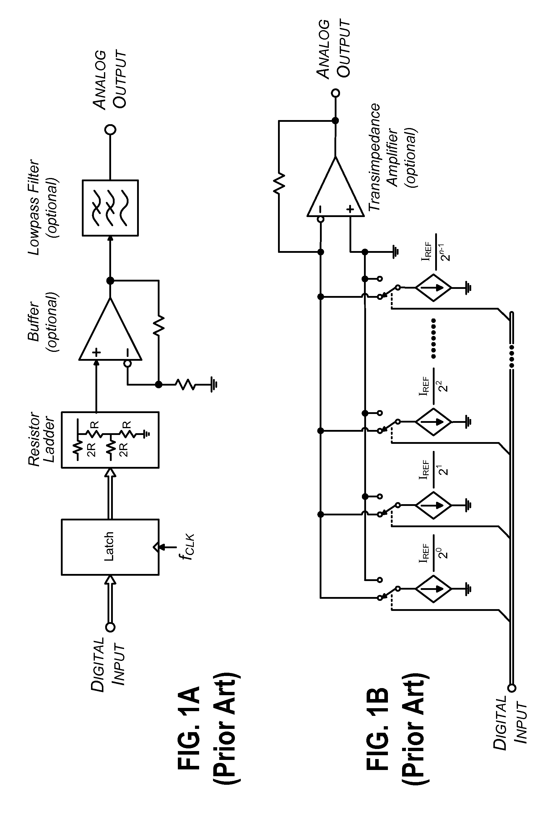
Conventional Nyquist converters potentially can achieve very high instantaneous bandwidths, but as discussed in greater detail below, the present inventor has discovered that component mismatches in the
resistor ladder network, or in the
switched current sources, can introduce
rounding errors that significantly limit attainable resolution.
In addition, the resolution of conventional Nyquist converters is limited by other practical implementation impairments such as sampling
jitter and thermal noise.
Although Nyquist converters potentially could realize
high resolution at instantaneous bandwidths greater than 10 GHz in theory, due to the foregoing problems, this potential has been unrealized in conventional Nyquist converters.
Increasing the
clock frequency fCLK of the ΔΣ modulator requires circuitry with higher speed capability, and generally,
higher power dissipation.
Increasing modulator order P, however, causes undesirable reductions in the stability of the modulator.
As a result of constraints on the
operating speed of conventional ΔΣ modulator circuits and on the
rounding accuracy of multi-level quantization circuits, increasing the
clock frequency and / or the order of the ΔΣ modulator has limited utility in improving the bandwidth and / or resolution of conventional
oversampling converters.
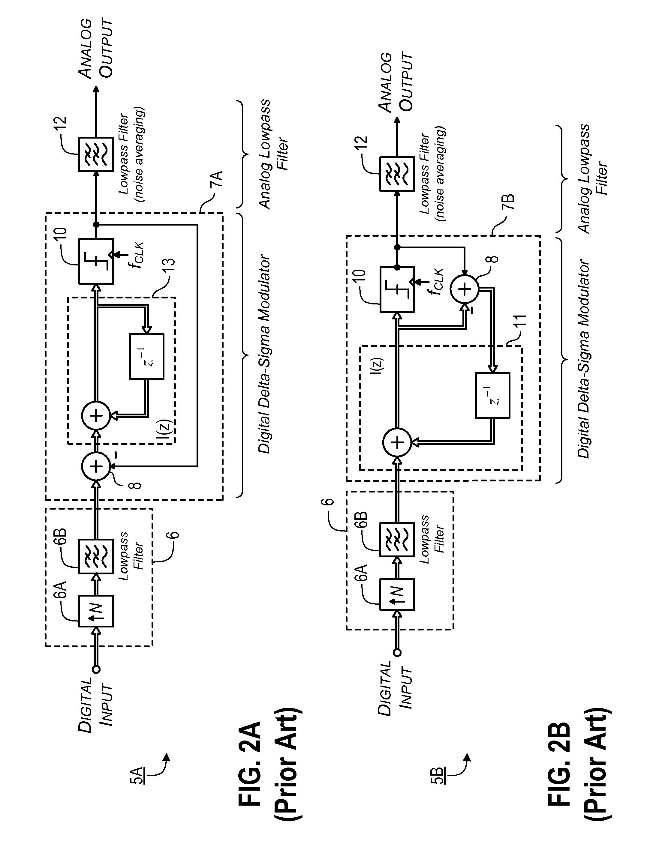
Although
oversampling with noise-shaped quantization can reduce quantization noise and other conversion errors, the output filtering (i.e.,
smoothing) operations generally limit the utility of oversampling converters to applications requiring only low
instantaneous bandwidth.
The present inventor has discovered that these conventional schemes for improving bandwidth and / or resolution in analog-to-
digital conversion suffer from significant disadvantages, particularly in attempts to directly adapt these schemes for use in digital-to-analog conversion applications.
However, the present inventor has discovered that the performance of this complementary scheme is limited by the
intermodulation distortion (i.e.,
intermodulation or non-ideal cross-products) of the analog mixers needed for the analog upconversion operation.
The present inventor, however, has discovered that the sampling rate (i.e., oversampling ratio) of this complementary scheme is limited by the switching times (speed) of the digital logic needed to implement the digital ΔΣ modulators (i.e., a less significant limitation in analog implementations).
Furthermore, the present inventor also has discovered that this complementary scheme is impractical because it requires a
bank of continuous-time analog filters whose individual responses replicate those of high-order, digital filters with
perfect reconstruction properties (i.e., a
bank of filters with an overall response that is all-pass).
Use of direct digital-to-analog filter transformations (i.e., those based on conventional bilinear or impulse-invariant transforms) to design analog filter banks with an all-pass response, generally results in analog filters of unmanageable complexity (i.e., filter orders of 30 or more).
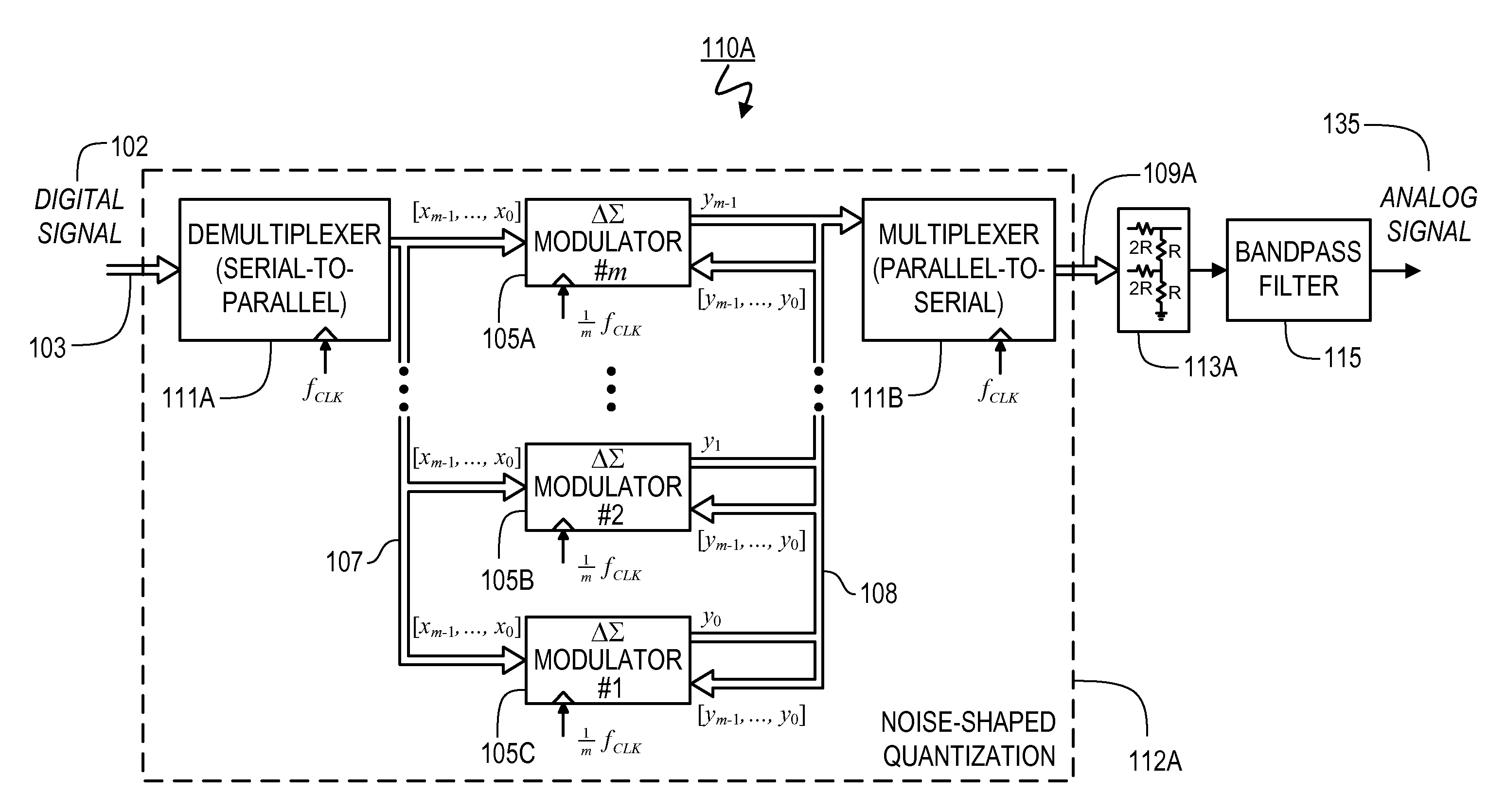
As discussed in greater detail below, simple replication and distribution of the difference and quantization functions (i.e., rather than
polyphase decomposition) causes conventional time-interleaved ΔΣ modulators to exhibit undesirable properties that prevent their use in very high-speed converter applications.
These disadvantages, which are discussed in greater detail in the Description of the Preferred Embodiment(s) section, include: 1) conversion bandwidth that is limited by the narrow lowpass or narrow
bandpass filtering operations used to attenuate shaped quantization noise and errors; 2) conversion resolution (SNDR) that is limited by the
clock frequency fCLK of the
delta-sigma modulator (i.e., the clock frequency of a two-level quantizer); and 3) conversion resolution that is limited by the low-order noise-shaped response (i.e., generally second-order for bandpass modulators) needed for stable operation with two-level quantizers.
In addition, conventional oversampling digital-to-analog converters cannot be operated in parallel as
hybrid filter banks (i.e., HFB scheme) or multi-band arrays (i.e., MBΔΣ scheme), without suffering from the amplitude and group
delay distortion introduced by imperfect analog filter banks, and / or the nonlinear (
intermodulation) distortion introduced by upconverting analog mixers.
Because of these disadvantages, the resolution of conventional oversampling converters cannot be increased without: 1) reducing bandwidth to improve the quantization
noise attenuation of the output (
smoothing) filters; or 2) increasing the converter sample rate by using digital circuits with higher switching speeds, since high-order modulators are unstable with two-level quantization.
In addition, conventional oversampling converters employ delta-sigma modulator structures that do not provide a means of dynamically varying, or re-
programming, the frequency (fnotch) at which the quantization noise
frequency response is a minimum.

