Semiconductor device, circuit substrate, and electronic device

a technology of semiconductor devices and electronic devices, applied in the field of semiconductor devices, can solve the problems of time and cost to commercialize what is called a system lsi, difficult to achieve further miniaturization, weight reduction, and more sophisticated functions, and achieve the effect of increasing the reliability of connection

Active Publication Date: 2012-10-30
ADVANCED INTERCONNECT SYST LTD
View PDF18 Cites 14 Cited by
  • Summary
  • Abstract
  • Description
  • Claims
  • Application Information

AI Technical Summary

Benefits of technology

[0014]An advantage of some aspects of the invention is to provide a semiconductor device that can increase the reliability of connection without increasing the area of apart where connection with an electrode pad is established and reliably form an insulation film on the inside wall surface of a through hole by finding an ingenious shape of an opening of a through electrode.
[0017]According to the semiconductor device with such a feature, both the electrode pad and the opening (the opening on the other surface side) located on the through hole side are rectangular. This makes it possible to make the area of the part joined to the electrode pad as large as possible and increase the reliability of connection of the through electrode without increasing the area of the joint part, that is, the area of the opening on the other surface side. Moreover, by making the opening on the other surface side narrower than the opening on the one surface side, a part which becomes a shadow from the opening on the one surface side to the opening on the other surface side is eliminated when an insulation film is formed on the inside wall surface of the through hole by CVD or the like. This makes it possible to form the insulation film reliably.Application Example 2

Problems solved by technology

Generally, it requires time and cost to commercialize what is called a system LSI.
In addition, a region where a device element such as a SAW (surface acoustic wave) element and an IC are mounted together has also become smaller and lighter, making it difficult to meet systematization.
However, it has been believed that the dependence on the wire bonding technique makes it difficult to achieve further miniaturization, weight reduction, and more sophisticated function.
Of the patent documents described above, the technique disclosed in Patent Document 1 may make it difficult to form an insulation film on the inside surface of a through hole, and an enlarged intermediate part of the through hole makes the technique unfit to obtain a layout configuration with a narrow pitch by miniaturization.
However, a large opening makes this technique also unfit to obtain a layout configuration with a narrow pitch by miniaturization.
The notch in an insulation film interface part becomes a shadow for the opening, making it difficult to form the insulation film on the inside wall surface of the through hole.
Moreover, since the amount of overetching varies depending on variations in the thickness of a Si substrate or variations in the etching rate, it is difficult to control the notch shape.
However, this method does not promise the effect thereof in a laminated substrate such as a laminated chip because, in such a laminated substrate, a surface to which a pulse is applied is not a subject to be etched.

Method used


Image

  • Semiconductor device, circuit substrate, and electronic device
  • Semiconductor device, circuit substrate, and electronic device
  • Semiconductor device, circuit substrate, and electronic device

Examples


Embodiment Construction

[0048]Hereinafter, an embodiment of a semiconductor device, a circuit substrate, and an electronic device of the invention will be described in detail with reference to the drawings.

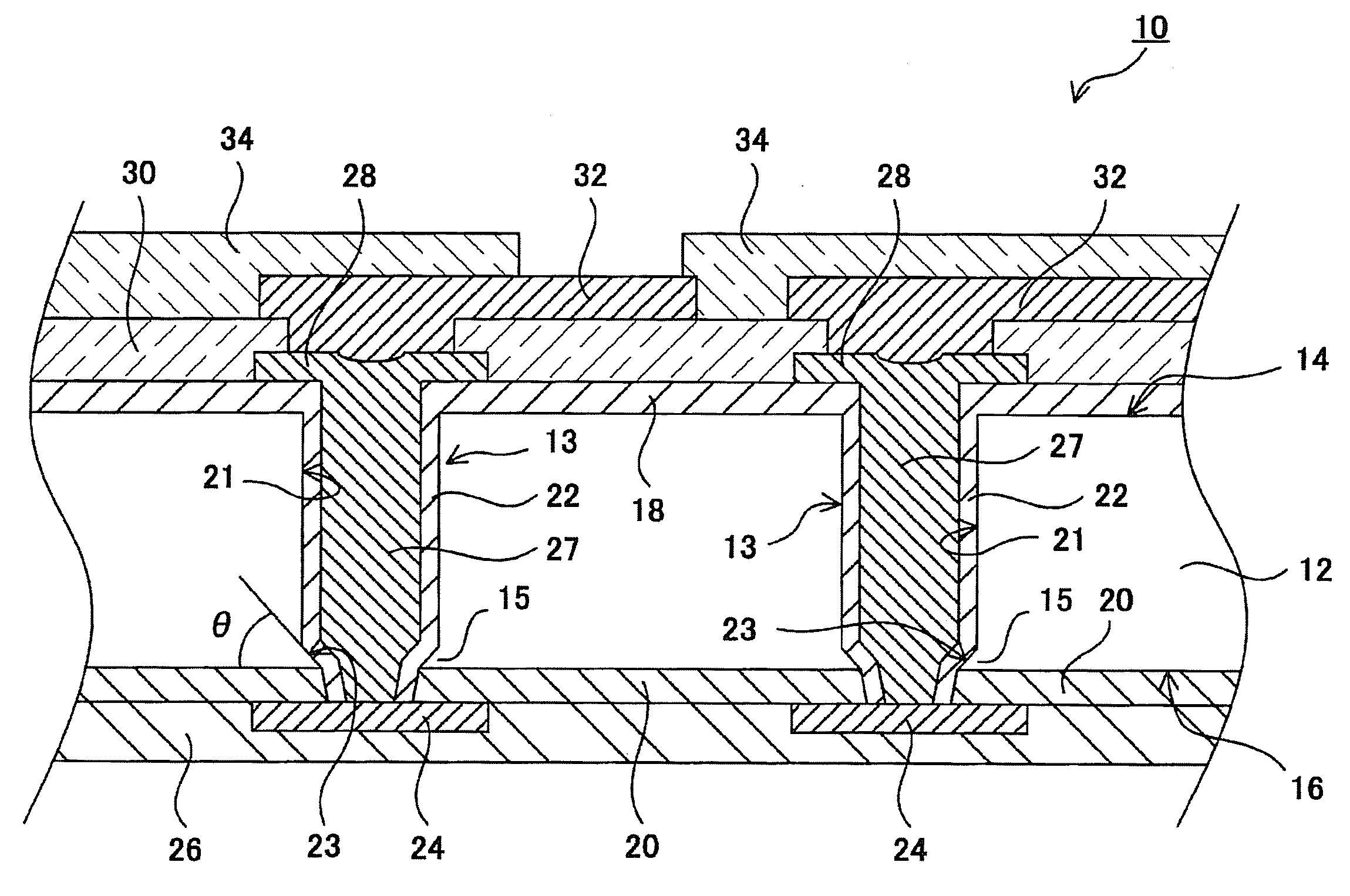
[0049]First, referring to FIG. 1, a first embodiment of the semiconductor device of the invention will be described. Incidentally, FIG. 1 is a partially enlarged sectional view showing principal portions of the semiconductor device according to the first embodiment.

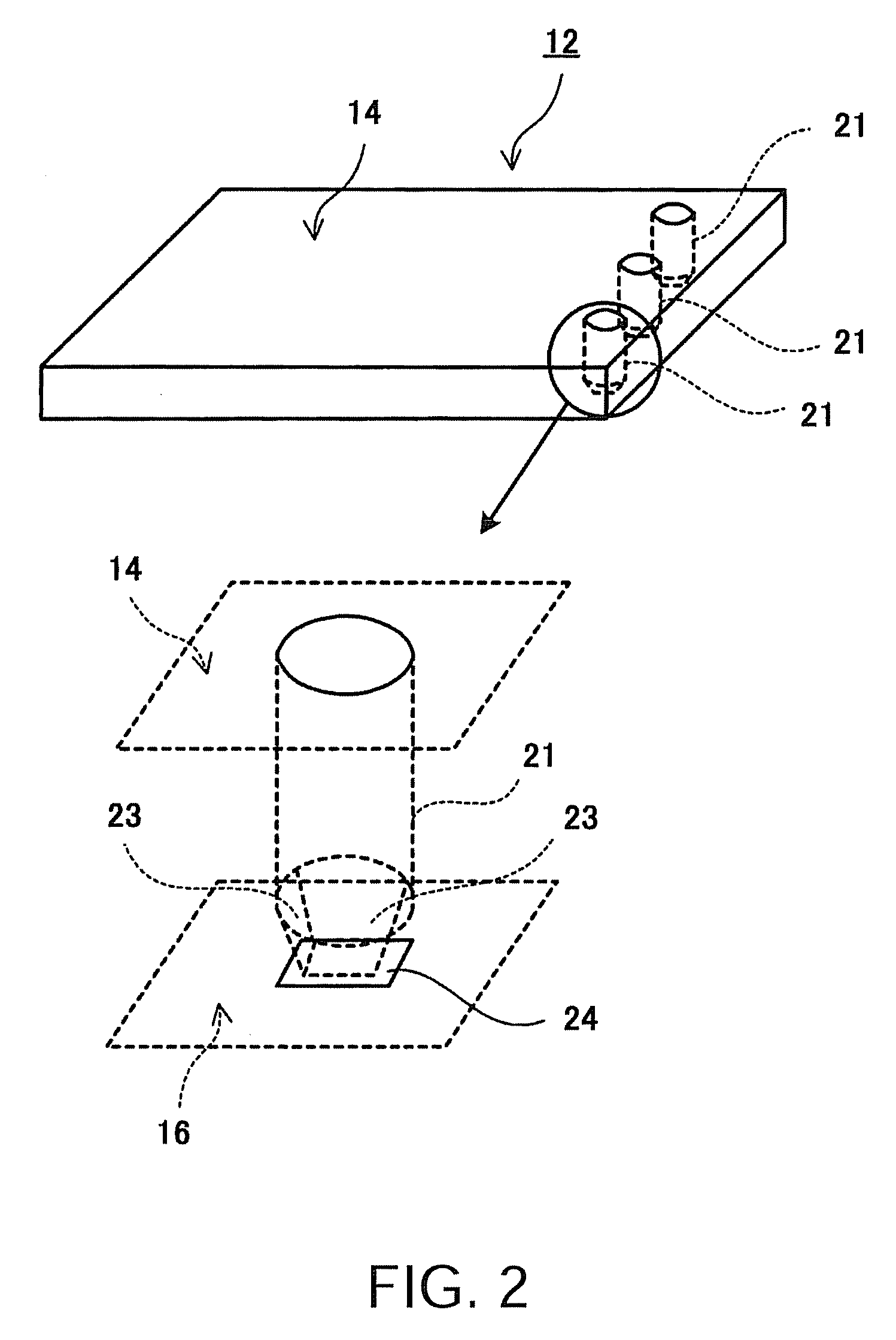
[0050]A semiconductor device 10 according to this embodiment includes, as basic portions thereof, a Si substrate 12, a through electrode (hereinafter referred to as a TSV) 13 provided in the Si substrate 12, and a rearrangement wiring layer 26 formed on an active face of an integrated circuit (not shown).

[0051]The Si substrate 12 is a substrate having a (100) face as a principal surface, and has one surface 14 and the other surface 16. On the one surface 14 and the other surface 16, insulation films 18 and 20 are respectively formed. The type ...


PUM


Abstract

A semiconductor device has a through electrode formed in a through hole which penetrates a Si substrate from one surface to the other surface of the Si substrate, wherein a rectangular electrode pad is provided on the other surface with an insulation film laid between the electrode pad and the other surface, an opening of the through hole on the one surface side is circular, an opening of the through hole on the other surface side is rectangular, and the area of the opening on the other surface side is made smaller than the area of the opening on the one surface side.

Description

BACKGROUND[0001]1. Technical Field[0002]The present invention relates to semiconductor devices and, in particular, to a semiconductor device having a through electrode formed therein, a circuit substrate incorporating the semiconductor device, and an electronic device incorporating the semiconductor device.[0003]2. Related Art[0004]Electronic information devices, as typified by cellular telephones, have become more compact and lighter, and the function thereof has become more sophisticated and faster. As a result, the IC which is the heart of such a device is also required to achieve miniaturization and weight reduction and to have more sophisticated function, and it is necessary to increase the added value thereof including shorter TAT (turn around time) and cost reduction.[0005]Generally, it requires time and cost to commercialize what is called a system LSI. In addition, a region where a device element such as a SAW (surface acoustic wave) element and an IC are mounted together h...

Claims


Application Information

Patent Timeline
Patent Type & Authority Patents(United States)
IPC IPC(8): H01L23/48H01L29/40H01L23/52
CPCH01L21/6835H01L21/76898H01L23/5384H01L23/481H01L2224/16H01L2221/68372
Inventor MATSUO, YOSHIHIDE
Owner ADVANCED INTERCONNECT SYST LTD
Why Eureka
Try Eureka