Pixel circuit, display system and driving method thereof

a pixel circuit and display system technology, applied in the field of display devices, can solve the problems of inability to display the desired image properly, the difference between the actual brightness of the pixels and the required brightness of some pixels specified by luminance data, and the non-uniformity of luminance of the amoled display, so as to reduce the threshold voltage shift and reduce the stress on the pixel circuit

Active Publication Date: 2012-10-30
IGNIS INNOVATION
View PDF42 Cites 12 Cited by
  • Summary
  • Abstract
  • Description
  • Claims
  • Application Information

AI Technical Summary

Benefits of technology

[0006]It is an object of the invention to provide a method and system that obviates or mitigates at least one of the disadvantages of existing systems.
[0008]According to another aspect of the present invention there is provided a pixel circuit that includes: a light emitting device; a driving transistor for driving the light emitting device, the driving transistor having a gate terminal, a first terminal coupled to the light emitting device, and a second terminal; a storage capacitor; a first switch transistor coupled to a data line for providing a programming data and the gate terminal of the driving transistor; and a second switch transistor for reducing a threshold voltage shift of the driving transistor, the storage capacitor and the second switch transistor being coupled in parallel to the gate terminal of the driving transistor and the first terminal of the driving transistor.
[0009]According to a further aspect of the present invention there is provided a method for a display having a pixel circuit. The pixel circuit has a light emitting device, a driving transistor for driving the light emitting device, and a storage capacitor. The method includes: at a first cycle, implementing an image display operation having programming the pixel circuit for a valid image and driving the light emitting device; and at a second cycle, implementing a relaxation operation for reducing a stress on the pixel circuit, including: selecting a relaxation switch transistor coupled to the storage capacitor in parallel, the storage capacitor being coupled to the gate terminal of the driving transistor and a first terminal of the driving transistor.

Problems solved by technology

However, the AMOLED displays exhibit non-uniformities in luminance on a pixel-to-pixel basis, as a result of pixel degradation.
There may be an ever-increasing error between the required brightness of some pixels as specified by luminance data and the actual brightness of the pixels.
The result is that the desired image will not show properly on the display.

Method used


Image

  • Pixel circuit, display system and driving method thereof
  • Pixel circuit, display system and driving method thereof
  • Pixel circuit, display system and driving method thereof

Examples


Embodiment Construction

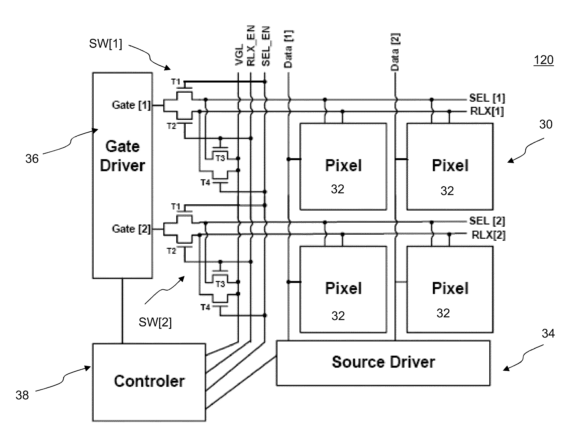
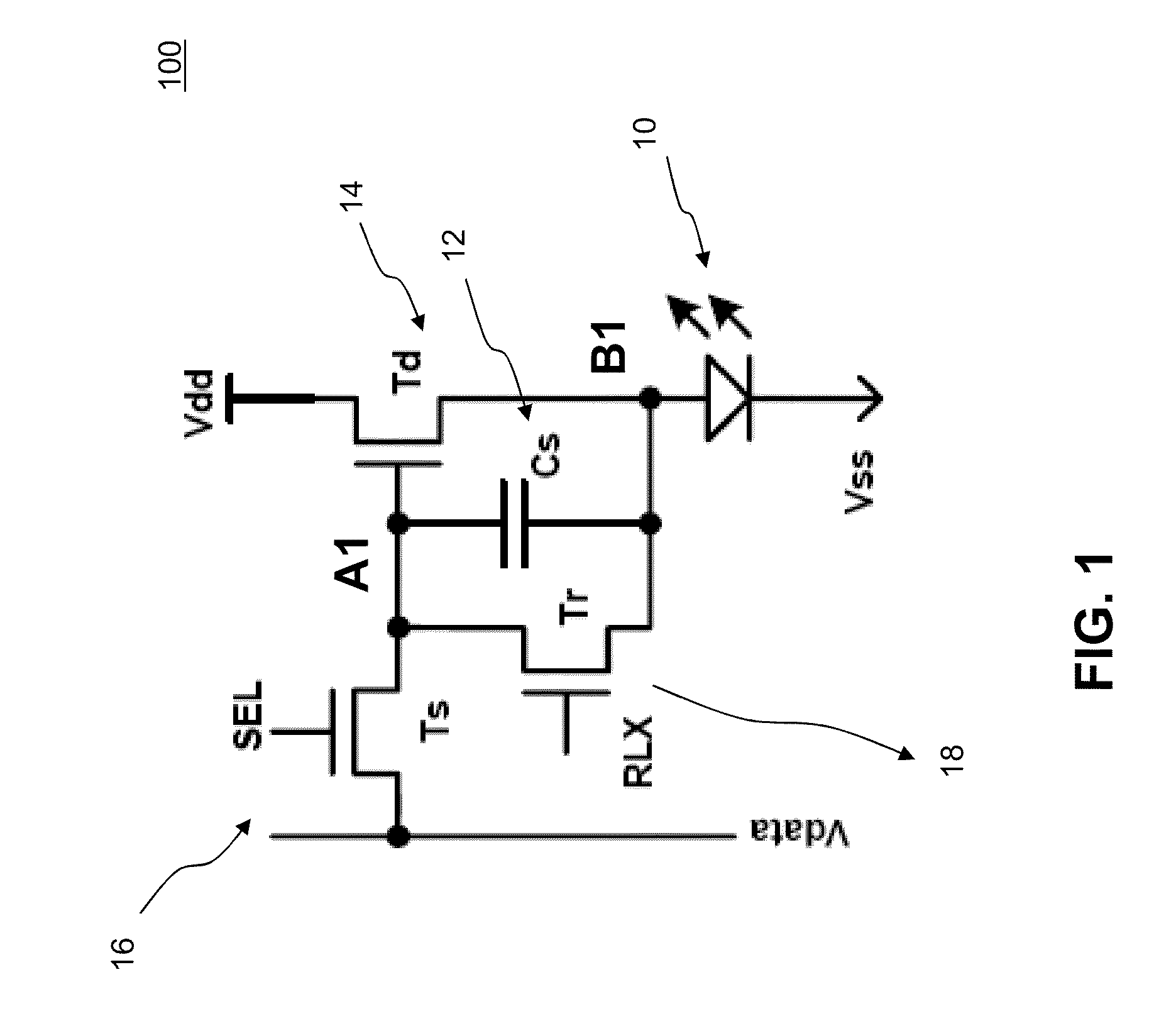
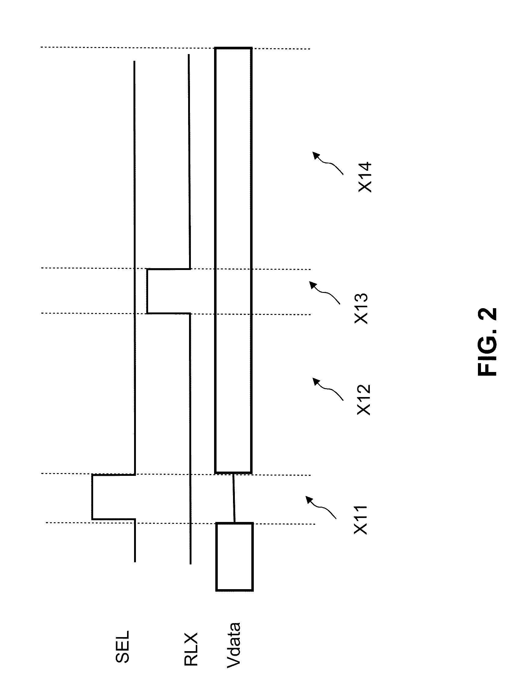
[0020]Embodiments of the present invention are described using an active matrix light emitting display and a pixel that has an organic light emitting diode (OLED) and one or more thin film transistors (TFTs). However, the pixel may include a light emitting device other than OLED, and the pixel may include transistors other than TFTs. The transistors of the pixel and display elements may be fabricated using poly silicon, nano / micro crystalline silicon, amorphous silicon, organic semiconductors technologies (e.g. organic TFTs), NMOS technology, CMOS technology (e.g. MOSFET), metal oxide technologies, or combinations thereof.

[0021]In the description, “pixel circuit” and “pixel” are used interchangeably. In the description, “signal” and “line” may be used interchangeably. In the description, “connect (or connected)” and “couple (or coupled)” may be used interchangeably, and may be used to indicate that two or more elements are directly or indirectly in physical or electrical contact wit...


PUM


Abstract

A display system and method for the same is provided. A display includes a plurality of pixels, each having a light emitting device and a driving transistor for driving the light emitting device, the driving transistor and the light emitting device being coupled in series between a first power supply and a second power supply. The method includes: at a first frame, programming a pixel with a first programming voltage different from a programming voltage for a valid image, and charging at least one of the first power supply and the second power supply so that at least one of the driving transistor and the light emitting device is under a negative bias. The pixel circuit includes: a light emitting device; a driving transistor for driving the light emitting device, the driving transistor having a gate terminal, a first terminal coupled to the light emitting device, and a second terminal; a storage capacitor; a first switch transistor coupled to a data line for providing a programming data and the gate terminal of the driving transistor; and a second switch transistor for reducing a threshold voltage shift of the driving transistor, the storage capacitor and the second switch transistor being coupled in parallel to the gate terminal of the driving transistor and the first terminal of the driving transistor. The method includes: at a first cycle, implementing an image display operation having programming the pixel circuit for a valid image and driving the light emitting device; and at a second cycle, implementing a relaxation operation for reducing a stress on the pixel circuit, including: selecting a relaxation switch transistor coupled to the storage capacitor in parallel.

Description

FIELD OF INVENTION[0001]The present invention relates to display devices, and more specifically to a pixel circuit, a light emitting device display and an operation technique for the light emitting device display.BACKGROUND OF THE INVENTION[0002]Electro-luminance displays have been developed for a wide variety of devices, such as, personal digital assistants (PDAs) and cell phones. In particular, active-matrix organic light emitting diode (AMOLED) displays with amorphous silicon (a-Si), poly-silicon, organic, or other driving backplane have become more attractive due to advantages, such as feasible flexible displays, its low cost fabrication, high resolution, and a wide viewing angle.[0003]An AMOLED display includes an array of rows and columns of pixels, each having an organic light emitting diode (OLED) and backplane electronics arranged in the array of rows and columns. Since the OLED is a current driven device, there is a need to provide an accurate and constant drive current.[0...

Claims


Application Information

Patent Timeline
Patent Type & Authority Patents(United States)
IPC IPC(8): G09G3/30H05B44/00G09G3/3208
CPCG09G3/3233G09G3/3291G09G2300/0819G09G2300/0842G09G2330/027G09G2310/0256G09G2320/043G09G2320/045G09G2320/048G09G2310/0254
Inventor NATHAN, AROKIACHAJI, G. REZADIONNE, J. MARCEL
Owner IGNIS INNOVATION
Why Eureka
Try Eureka