Bus controller arranged between a bus master and a networked communication bus in order to control the transmission route of a packet that flows through the communication bus, and simulation program to design such a bus controller

bus controller technology, applied in the field of apparatus, method and program for controlling a networked communication bus, can solve the problems of increasing the number of bus masters connected to the communication bus on the chip, increasing the complexity of traffic control on transfer data being transmitted and received through the bus, and causing wiring delays. to achieve the effect of eliminating such non-uniform data flow ra

Active Publication Date: 2012-10-30
PANASONIC CORP
View PDF11 Cites 0 Cited by
  • Summary
  • Abstract
  • Description
  • Claims
  • Application Information

AI Technical Summary

Benefits of technology

[0024]It is therefore an object of the present invention to provide a bus controller that can eliminate such non-uniformity in data flow rate between those links.
[0030]The route load detecting section may adjust the parameter defining the degree of reliability by sensing a deterioration in the transfer status of the packet. Unless the transfer status improves even by adjusting the parameter, the route load detecting section may make a probability-based adjustment on the parameter.
[0037]The bus controller of the present invention monitors the output status with respect to other bus controllers that exist on multiple transmission routes available, and changes the data transmission routes based on the uniformity of distribution index indicating the degree of non-uniformity in transmission flow rate between the respective transmission routes. Thus, the degree of non-uniformity in flow rate between the links that form an NoC bus can be reduced automatically. As a result, the data transfer load can be distributed more uniformly over the entire bus. Consequently, an increase in communication delay or latency, which would otherwise be caused by an excessively heavy traffic on a particular link, can be minimized.
[0038]In addition, since the operating frequencies of the links can be lowered, the bus can be designed more easily and the power dissipation of the bus while data is being transferred can be cut down. Optionally, by combining this technique with a technique for dynamically controlling the operating frequencies of the links, the power dissipation of the bus can be cut down even more efficiently.
[0039]On top of that, by making the route loads on other bus masters that have a similar function more uniform in view of the statistical multiplexing effect, the loads on those bus masters can be distributed more uniformly as well. That is why by applying the present invention to a distributed memory architecture, a bottleneck that would otherwise be caused by excessive access can be avoided with a sufficient degree of reliability ensured in terms of allowable memory access latency.

Problems solved by technology

And as the performance of a semiconductor chip has been enhanced these days to meet such a demand, the number of bus masters to be connected to the communication bus on the chip has been increasing and the traffic control to be done on transfer data being transmitted and received through the bus has getting more and more complicated.
According to such a bus control method, a wiring delay will be caused because the bus needs to circumvent the circuit board.
In addition, since the cross-bar switches have to be arranged, an additional area needs to be left for them and the power dissipation also increases by using such switches.
Likewise, if the frame transfer latency on the data transfer route currently chosen is too long for the frame to arrive at the receiving end within a predetermined period of time, the bus master on the transmitting end cannot receive the acknowledge data within the predetermined time.
Such non-uniformity causes the following three problems.
First of all, in a link with a high flow rate, the operational loads on bus controllers at both ends of that link become so heavy that the data transfer latency increases significantly.
For example, when data is transferred between a processor and a memory, the memory access latency increases the overall length of wait cycles for the processor, which will lead to a decline in performing performance.
However, the higher the operating frequency of the bus, the more difficult it is to control the wiring delay and the crosstalk and the greater the number of design or verification process steps.
Thirdly, the higher the operating frequency of the bus, the greater the power dissipated by a link.
That is why depending on the degree of non-uniformity of the flow rate, the power dissipation of the link that should cope with a high transfer rate could be very large.

Method used


Image

  • Bus controller arranged between a bus master and a networked communication bus in order to control the transmission route of a packet that flows through the communication bus, and simulation program to design such a bus controller
  • Bus controller arranged between a bus master and a networked communication bus in order to control the transmission route of a packet that flows through the communication bus, and simulation program to design such a bus controller
  • Bus controller arranged between a bus master and a networked communication bus in order to control the transmission route of a packet that flows through the communication bus, and simulation program to design such a bus controller

Examples


embodiment 1

[0071](Embodiment 1)

[0072]Before a bus controller as a first preferred embodiment of the present invention is described in detail, a so-called “NoC (Network on Chip)” communication bus, transmission routes that can be used on the communication bus, and the data transfer rates of the respective transmission routes will be described. In addition, it will also be described how in principle the bus controller of this preferred embodiment operates.

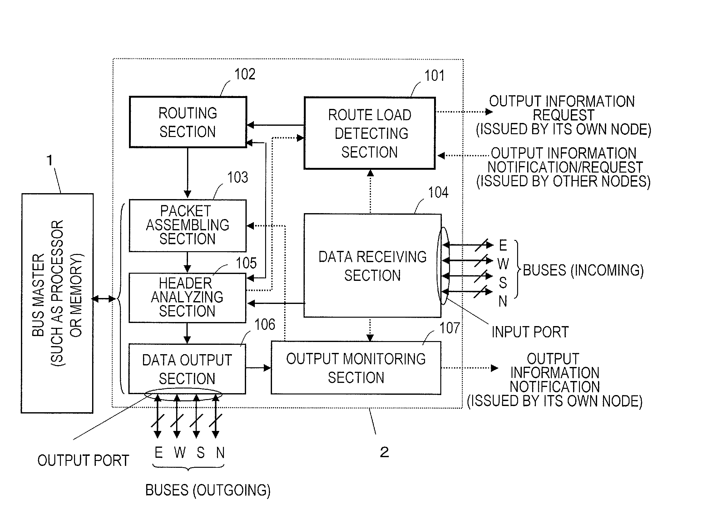
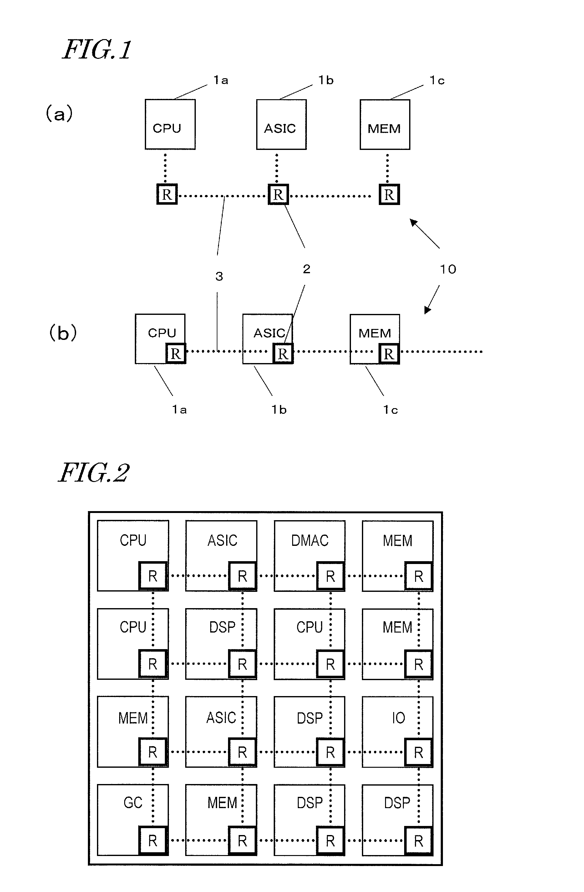
[0073]FIG. 5 illustrates how a system on chip semiconductor LSI to be built in cellphone terminals, for example, may be formed using an NoC bus. This drawing is also illustrated in the same format as FIG. 1(b). Although a bus controller R is connected one to one to each single bus master in FIG. 5, some bus controllers may just perform a relay function without being connected to any bus master.

[0074]If each bus controller R is connected to its associated bus master, each bus master is given a non-ambiguous address. On the other hand, if not eve...

embodiment 2

[0156](Embodiment 2)

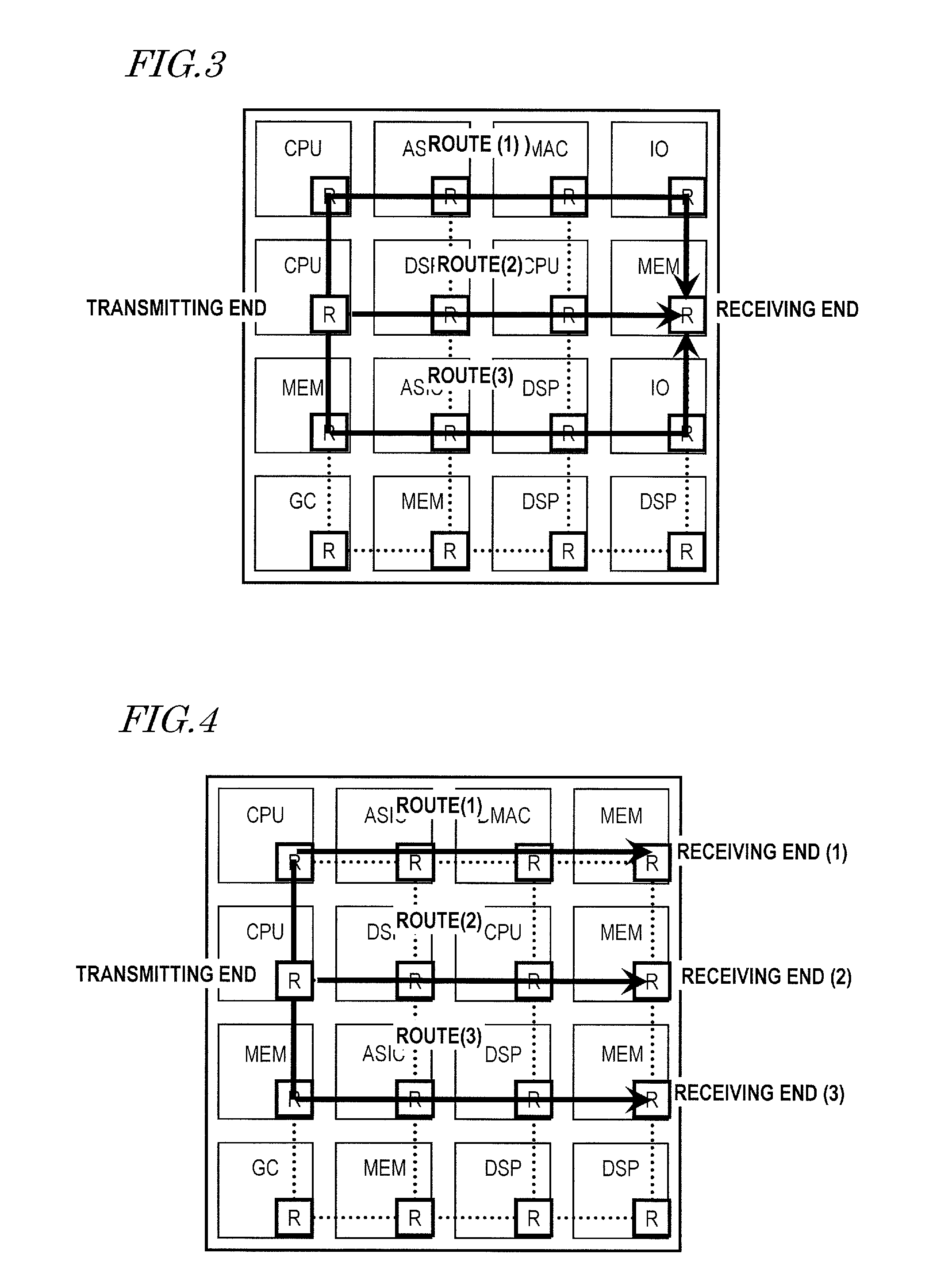
[0157]FIG. 20 illustrates an exemplary configuration in which the present invention is applied to a distributed memory architecture. In this arrangement, three processors UP11, UP12 and UP13 and three shared memory modules MEM31, MEM32 and MEM33 are connected together with a network of bus controllers that is implemented as a 3×3 mesh. Each of these processors allocates a memory space that is required when a task is started to one of these memory modules, and frees that memory space when the task gets done. However, if the memory spaces were allocated to a particular memory module so often, the access rates would be non-uniform between the memory modules, and the operating frequency on the access bus leading to that particular memory module would increase due to the excessive access, thus causing problems in terms of design and power dissipation. However, if the processor carries out the memory space allocation so that the access rates will be as uniform as possi...

embodiment 3

[0191](Embodiment 3)

[0192]A bus controller as a third specific preferred embodiment of the present invention is also applicable to the distributed memory architecture shown in FIG. 20 as in the second preferred embodiment of the present invention described above. However, as such a distributed memory architecture has already been described for the second preferred embodiment, the description thereof will be omitted herein.

[0193]Each of the bus controllers that form the distributed memory network of this preferred embodiment has the same configuration as the bus controller 2 of the second preferred embodiment shown in FIG. 14 except the following respects. Thus, description of their common features will be omitted herein.

[0194]Route Load Detecting Section 101

[0195]In this preferred embodiment, Equation (16) adopted in the second preferred embodiment described above may be replaced with the following Equation (24):

[0196]ρi={1(max⁢{β^i}=0)min⁢{β^i}max⁢{β^i}(otherwise)(24)

[0197]It is de...


PUM


Abstract

A bus controller includes: a data receiving section for receiving output status information from other bus controllers on transmission routes available; a route load detecting section for calculating uniformity of distribution index indicating the degree of non-uniformity in transmission flow rate between the routes based on the output status information; a routing section for determining transmission routes, of which the transmission flow rates have been adjusted by reference to the index; a packet assembling section for generating a packet; a data output section for outputting the packet through one of output ports; a header analyzing section for determining which output port is connected to a transmission route chosen by reference to information about the packet receiving end; and a data output section for outputting the packet through the output port.

Description

[0001]This is a continuation of International Application No. PCT / JP2010 / 004290, with an international filing date of Jun. 29, 2010, which claims priority of Japanese Patent Applications No. 2009-161029, filed on Jul. 7, 2009, and No. 2009-234538, filed on Oct. 8, 2009, the contents of which are hereby incorporated by reference.BACKGROUND OF THE INVENTION[0002]1. Field of the Invention[0003]The present invention relates to an apparatus, method and program for controlling a networked communication bus for use in a semiconductor chip.[0004]2. Description of the Related Art[0005]Recently, in the fields of built-in computers and general-purpose processors that use an SoC (System on Chip), there is a growing demand for semiconductor chips with enhanced performance. And as the performance of a semiconductor chip has been enhanced these days to meet such a demand, the number of bus masters to be connected to the communication bus on the chip has been increasing and the traffic control to b...

Claims


Application Information

Patent Timeline
Patent Type & Authority Patents(United States)
IPC IPC(8): G06F13/00H04L12/721H04L12/803H04L12/701H04L12/851
CPCH04L12/40019
Inventor ISHII, TOMOKIYAMAGUCHI, TAKAOYOSHIDA, ATSUSHI
Owner PANASONIC CORP
Why Eureka
Try Eureka