
Device and a method of manufacturing a housing material

a manufacturing method and technology applied in the field of devices and a manufacturing method of a housing material, can solve the problems of not offering the hardness, corrosion resistance, appearance, other surface properties, and material not practical for use as a case member, and achieve the effect of easy processing, excellent freedom of product design, and easy reduction of product siz

Active Publication Date: 2012-11-06
SEIKO EPSON CORP
View PDF37 Cites 13 Cited by
  • Summary
  • Abstract
  • Description
  • Claims
  • Application Information

AI Technical Summary

Benefits of technology

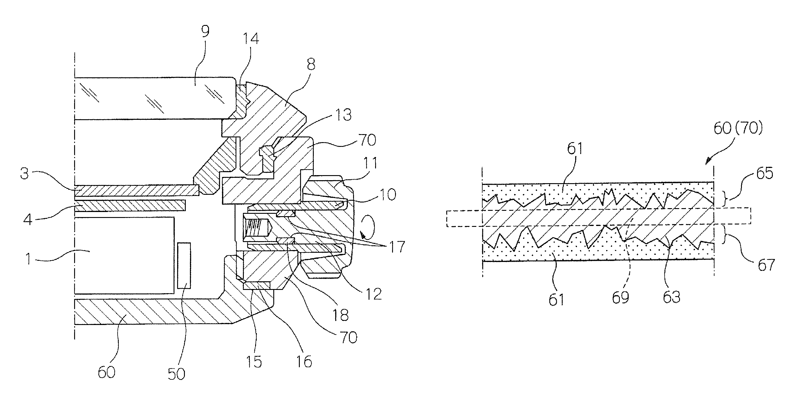
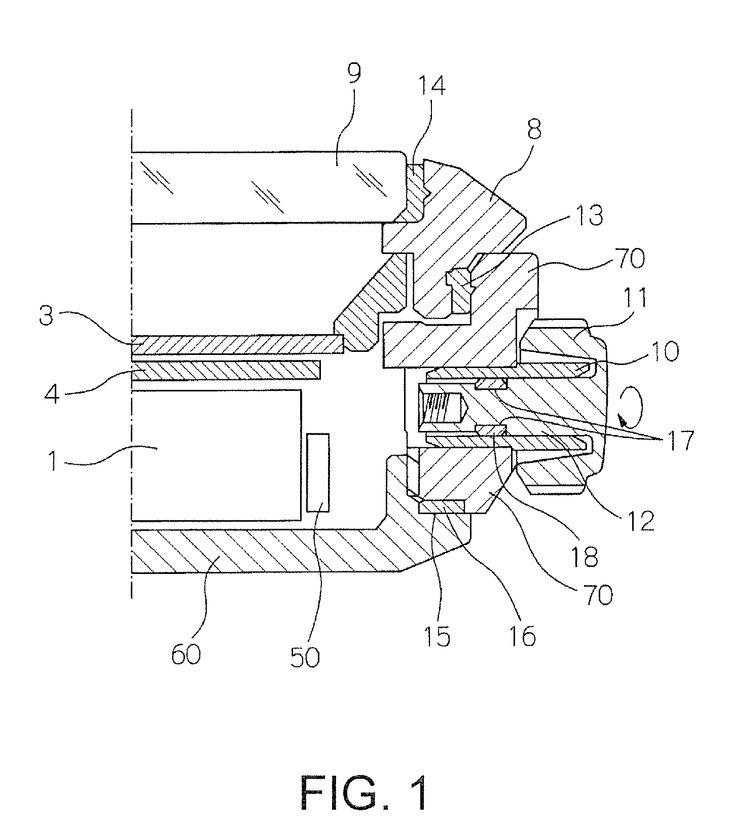
[0013]By using a housing that can be easily processed, provides the hardness, corrosion resistance, appearance, and other surface characteristics required for a case member component, and functions sufficiently as a magnetic shield for magnetically shielded components such as a timepiece movement, the invention eliminates the need for a dedicated magnetic shield member in a timepiece or other device, thereby enabling easily reducing product size, while also affording excellent freedom of product design.

Problems solved by technology

However, because a ferritic material is used, the resulting components do not offer the hardness, corrosion resistance, appearance, and other surface properties that are most important in a timepiece case member.
More specifically, this material is not practical for use as a case member.
However, because austenitic stainless steel is difficult to process, processing austenitic stainless steel to the desired shape is difficult and manufacturing costs therefore rise.
However, these methods simply teach technology for using ferritic stainless steel to produce case member parts of the desired shape from ferritic stainless steel, and then austenitize the surface using nitrogen gas in order to achieve the strength, corrosion resistance, and other surface properties desired in a case member, and are silent regarding the internal structure of the ferrite phase after the austenitizing process.
As a result, the nitrogen concentration is also not uniform, and the interface between the austenitized parts of the surface layer and the ferritic phase of the internal layer left below is particularly uneven.
In this case a uniform ferrite layer cannot be maintained and the internal ferrite phase layer may not be contiguous.
More simply, the resulting part is unsuitable for use as a magnetic shield.
The speed at which the nitrogen penetrates the ferrite phase is not uniform and varies by location.
As a result, the nitrogen concentration is also not uniform and the boundary between the austenitized surface layer portion and the ferrite phase internal layer portion is particularly uneven.
In this case a uniform ferrite layer cannot be maintained and the internal ferrite phase layer may not be contiguous.
More particularly, because the movement is a dense assembly of precision mechanical parts, the ability to further reduce the size of the movement itself is already near the practical limit.
This is because the production of chromium nitride reduces the nitrogen concentration in that part, and the austenite phase at the inside portion where the nitrogen concentration drops becomes unstable changes to ferrite phase.

Method used


Image

  • Device and a method of manufacturing a housing material
  • Device and a method of manufacturing a housing material
  • Device and a method of manufacturing a housing material

Examples


example 1

[0123]A housing component, specifically the back cover of a timepiece, was manufactured using the method described below.

[0124]A ferritic stainless steel substrate made from an Fe—Cr alloy of primarily Fe was prepared. The composition of this substrate was Fe, 18.3 wt % Cr, 2.25 wt % Mo, 0.15 wt % Nb, 0.26 wt % Mn, 0.006 wt % C, 0.001 wt % S, 0.022 wt % P, 0.21 wt % Si, and was primarily ferrite phase. The content of any element also contained as an unavoidable impurity was less than 0.001 wt %.

[0125]This substrate was then forged to produce a substrate with the desired shape of the back cover for a wristwatch, and was then ground and polished as needed.

[0126]The substrate was then washed. The substrate was first washed by alkaline electrolytic degreasing for 30 seconds followed by alkaline immersion degreasing for 30 seconds. The substrate was then neutralized for 10 seconds, washed in water for 10 seconds, and then washed in demineralized water for 10 seconds.

[0127]An austenitizin...

examples 2 to 7

[0134]Examples 2 to 7 differed from the first example described above only in the composition of the Fe—Cr alloy ferritic stainless steel used for the substrate and the conditions of the austenitizing process as shown in Table 1. Other than these differences, back covers for a wristwatch were manufactured in the same way as described in example 1 above.

[0135]Comparison 1

[0136]Other than not applying the austenitizing process, the back cover for a wristwatch according to this first comparison sample was manufactured in the same way as the first example described above. More specifically, the back cover resulting from the forging process was used as the back cover of the wristwatch.

[0137]Comparison 2

[0138]The back cover of a wristwatch was manufactured by the process described below.

[0139]A ferritic stainless steel metal powder (primarily Fe with a composition of Fe, 21.63 wt % Cr, 2.28 wt % Mo, 0.12 wt % Nb, 0.06 wt % S, 0.45 wt % Mn, 0.8 wt % Si, 0.018 wt % P, 0.04 wt % C) was prepa...


PUM

PropertyMeasurementUnit
thickaaaaaaaaaa
thicknessaaaaaaaaaa
thicknessaaaaaaaaaa

Abstract

A device has a magnetically shielded component that is magnetically shielded from an external magnetic field, and a housing. The housing is made from a ferritic stainless steel that has an austenitized surface layer rendered on the surface, and an internal layer portion having an internal ferrite phase that functions as a magnetic shield for the magnetically shielded component.

Description

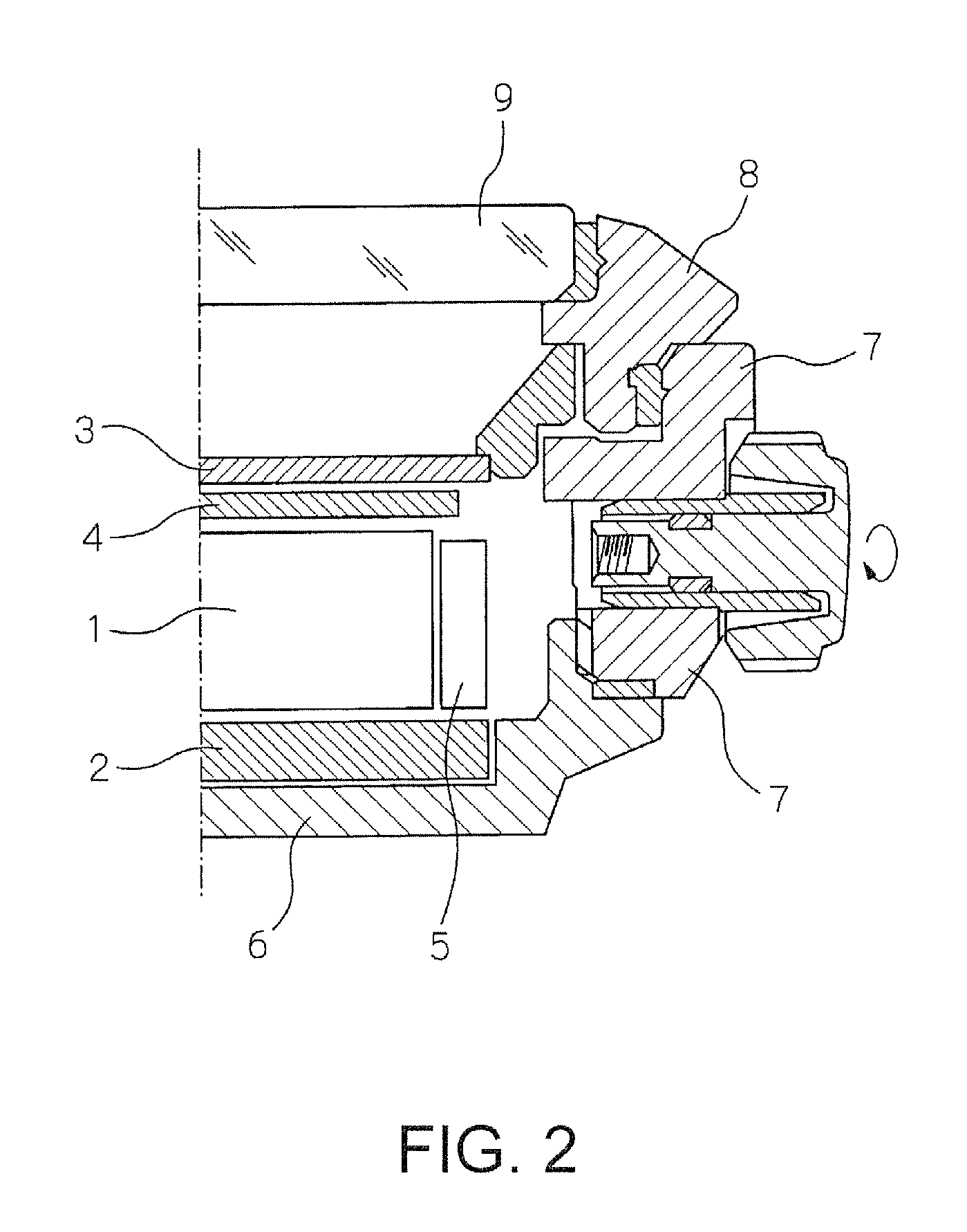
BACKGROUND[0001]1. Field of Invention[0002]The present invention relates to a device such as a timepiece that has a housing and a magnetically shielded component that is magnetically shielded from an external magnetic field, and to a method of manufacturing a housing material used as an external component of the device.[0003]2. Description of Related Art[0004]Stepping motors that have an electromagnet made from a drive coil and a stator, a rotor made from a permanent magnet, and use the repulsion of the electromagnet and rotor to drive the rotor are commonly used in timepiece movements to drive the hands in modern electronic timepieces. Such movements may cease operating normally when exposed to a strong external magnetic field. The movement is therefore covered with a dedicated magnetic shield. A structure with this dedicated magnetic shield according to the related art is shown in FIG. 2, but the structure is described in detail in contrast to a preferred embodiment of the inventi...

Claims


Application Information

Patent Timeline
Patent Type & Authority Patents(United States)
IPC IPC(8): G04B37/00A44C5/00C22C38/18C23C8/00C23C8/50C21D1/06C21D9/00C22C38/00C22C38/48C23C8/26G04B37/22G04B43/00G04C3/00G04G17/08G04G21/04
CPCG04B43/00G04G17/08
Inventor TAKASAWA, KOKI
Owner SEIKO EPSON CORP
Learn More