Circuit module and power line communication apparatus

a technology of circuit modules and power lines, applied in the field of circuit modules, can solve the problems of increasing the thickness of laminated boards, wasting mounting and wiring space, and reducing processing accuracy, so as to achieve high reliability, maintain processing accuracy, and avoid noise.

Inactive Publication Date: 2012-11-13
PANASONIC CORP
View PDF37 Cites 2 Cited by
  • Summary
  • Abstract
  • Description
  • Claims
  • Application Information

AI Technical Summary

Benefits of technology

[0007]The present invention is provided to address the above-described problems. An object of the present invention is to provide a compact circuit module being hardly affected by noise and having high reliability. Another object of the present invention is to provide a compact, low-noise, and high-speed power line communication apparatus.
[0008]A circuit module explained in the embodiments below has a laminated board and an IC; the laminated board having a first insulating layer, a first conductive layer laminated on the first insulating layer, a second insulating layer laminated on the first conductive layer, and a second conductive layer laminated on the second insulating layer; the IC being mounted on the first insulating layer and having a plurality of ground terminals. The first conductive layer is electrically connected to the plurality of ground terminals. The above-described structure provides a minimum distance between the ground terminals and a ground layer and connects the ground terminals and the ground layer while requiring no via hole that penetrates the laminated board and maintaining processing accuracy. Thereby, a mounting space is not reduced on a rear surface of the laminated board, the rear surface being a surface on which no IC is mounted. Further, an increase in inductance is minimized, which is caused by an increased thickness of the laminated board. The conductive layer provided proximate to the IC herein is a proximate layer, except a conductive layer that configures a wiring pattern as a connection pad on the laminated board surface.
[0009]Further, a circuit module explained in the embodiments below has a laminated board and an IC; the laminated board having a first insulating layer, a first conductive layer laminated on the first insulating layer, a second insulating layer laminated on the first conductive layer, and a second conductive layer laminated on the second insulating layer; the IC having a plurality of ground terminals and processing a high-frequency signal. The IC is mounted on the first insulating layer, and the plurality of ground terminals are electrically connected to the first conductive layer. The above-described structure provides a minimum distance between the ground terminals and a ground layer and connects the ground terminals and the ground layer while requiring no via hole that penetrates the laminated board and maintaining processing accuracy. Thereby, a mounting space is not reduced on a rear surface of the laminated board, the rear surface being a surface on which no IC is mounted. Further, an increase in inductance is minimized, which is caused by an increased thickness of the laminated board, thereby preventing attenuation of the high-frequency signal processed by the IC. The conductive layer provided proximate to the IC herein is a proximate layer, except a conductive layer that configures a wiring pattern as a connection pad on the laminated board surface.

Problems solved by technology

However, such a deep through-via requires a large planar space and a space on a rear side, thus wasting the mounting and wiring spaces.
There is a problem, however, where the farther the ground layer is provided from the ground terminal of modulation / demodulation IC 2100, the more the processing accuracy declines.
In addition, the increase in inductance caused by the increased thickness of the laminated board is more than a small problem, as described above.

Method used


Image

  • Circuit module and power line communication apparatus
  • Circuit module and power line communication apparatus
  • Circuit module and power line communication apparatus

Examples


first embodiment

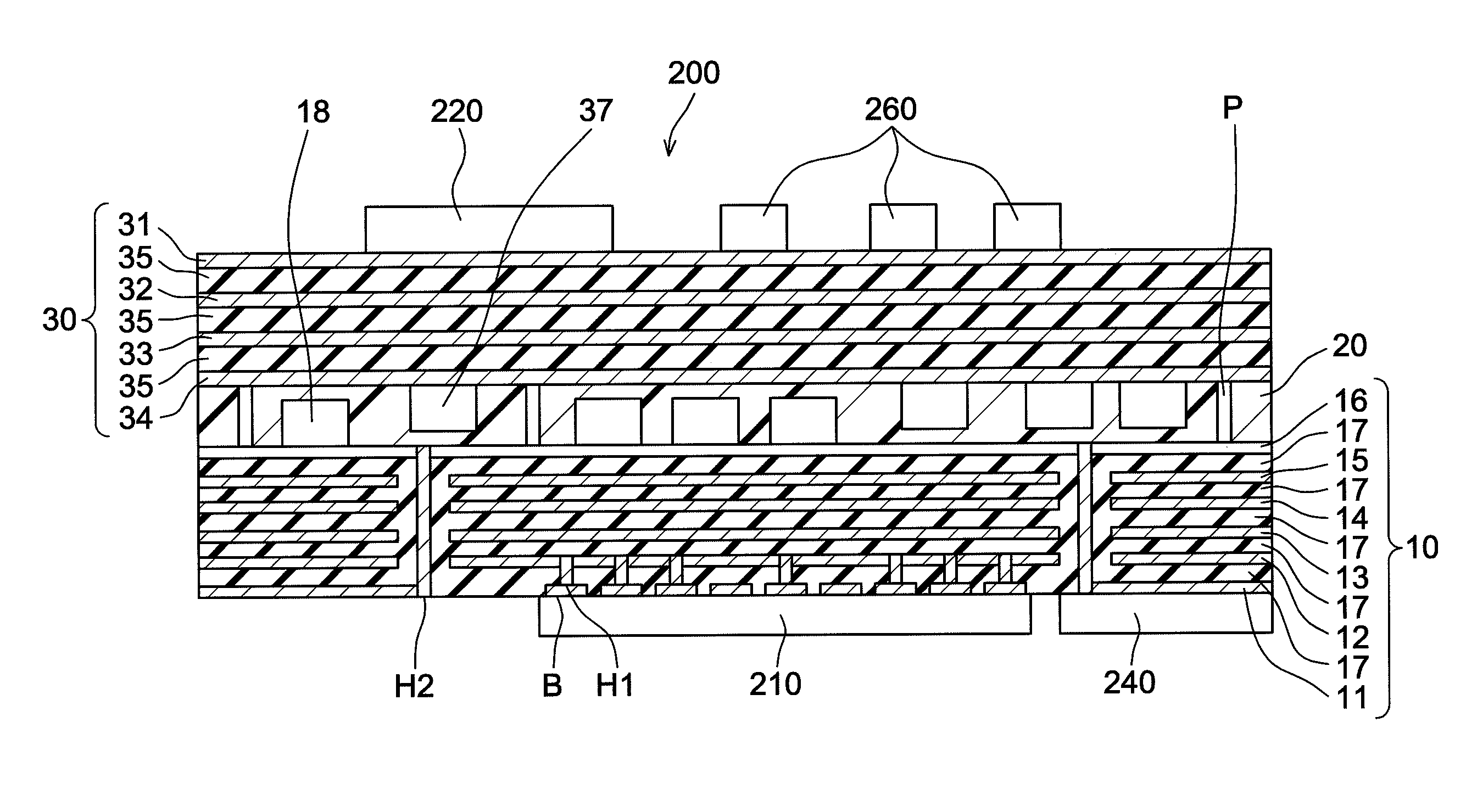
[0031]Explained in a first embodiment is PLC modem 100, as an IC mounting board, which stores in case 101 a PLC board used for high-speed power line communication (PLC). PLC modem 100 is an example of a PLC apparatus, which may be an electrical apparatus having a PLC modem therein.

[0032]In the first embodiment, PLC circuit module 200 includes two IC mounting boards as shown in FIGS. 1 and 2. More specifically, in first laminated board 10, which is one of the two IC mounting boards that configure PLC circuit module 200 mounted in PLC modem 100, first metal layer 12 is a conductive layer provided proximate to modulation / demodulation IC 210 as an IC, and is electrically connected to a ground terminal of modulation / demodulation IC 210.

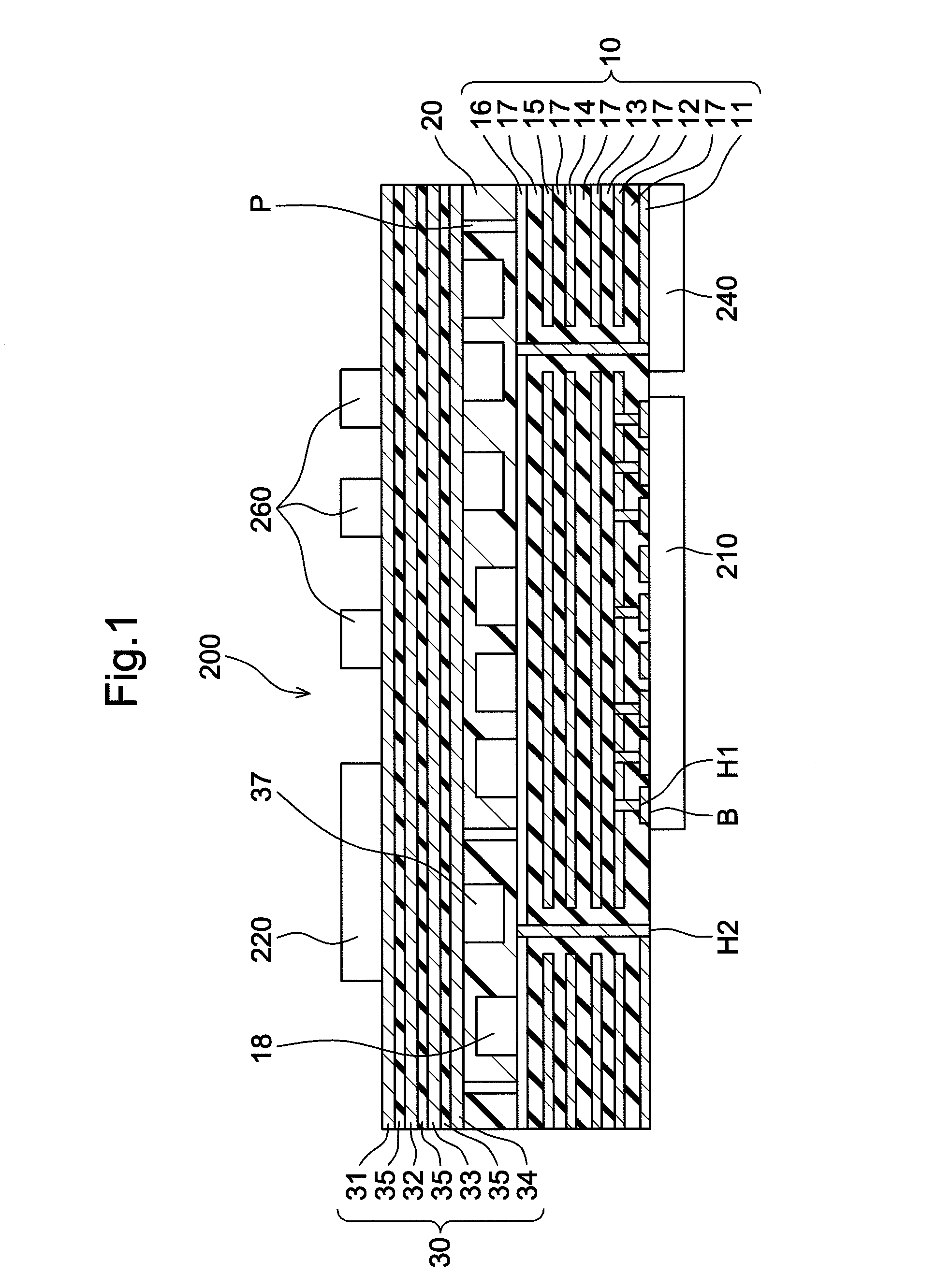
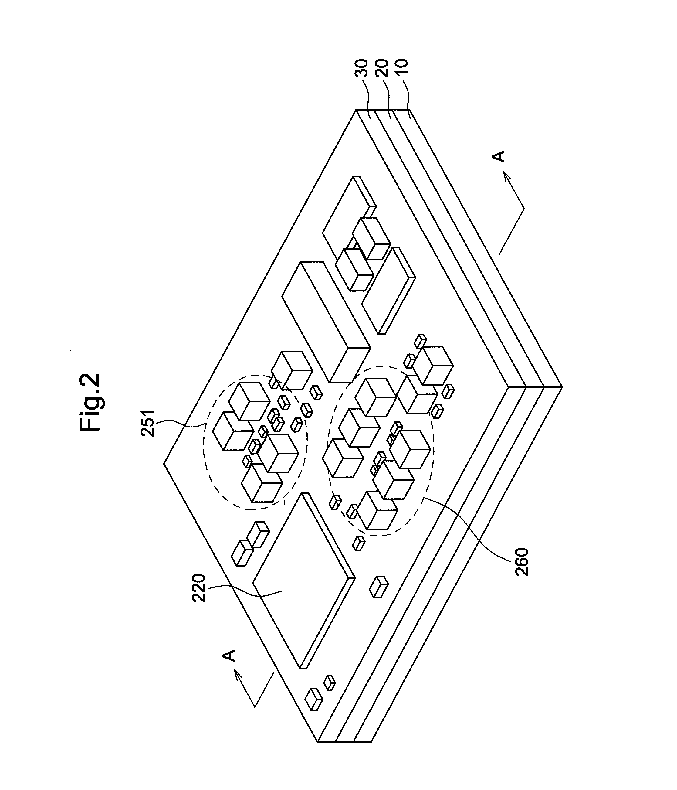
[0033]As shown in FIGS. 1 and 2 (FIG. 1 is a sectional view of section A-A of FIG. 2), first laminated board 10 is fixatedly attached to second laminated board 30 having therebetween composite sheet 20 as an insulating sheet, in the first embodiment. First...

second embodiment

[0090]A second embodiment is explained below. As shown in a sectional view in FIG. 13 and in a perspective view in FIG. 14, laminated board 10 as an IC mounting board according to the second embodiment is mounted with balanced filter 260 on a surface contacting a composite sheet between two laminated boards. Balanced filter 260 is surrounded along a circumference thereof by conductive pillars Q having conductive paste and providing conductive paths. Since similar processing is performed in processes of a manufacturing process of a PLC module in FIGS. 10C and 10D, man-hour can be minimized. Thereafter, the IC mounting board is provided in a similar manner to an IC mounting board shown in FIG. 1.

[0091]In the present embodiment, balanced filter 260 is mounted in insulating sheet 20 and is surrounded by conductive pillars Q having copper foil and conductive paste. Thereby, an impact of noise can be minimized and a compact and affordable module unaffected by a mounting environment can be...

third embodiment

[0094]A third embodiment is explained below. In the third embodiment, a PLC module has a structure where heat-dissipating metal layers 40 and 41 are laminated onto upper and lower surfaces of the PLC module obtained in the above-described first embodiment, having composite sheets 42 and 43 respectively in between as shown in FIG. 15, thus allowing effective heat dissipation as the module. Other components are provided in a similar manner to the PLC module according to the first embodiment shown in FIG. 1. Same reference numbers are provided to the same components. The structure above having the heat-dissipating plates on both the upper and lower surfaces expands a heat-dissipating space even when the circuit density increases, and provides a compact and affordable module. Described herein is a case where there are two heat-dissipating metal plates, but one metal plate may be used. For instance, providing the metal plate only to an IC having the largest heat generation (e.g., a main ...


PUM


Abstract

A circuit module is mounted with an IC that modulates and demodulates a multicarrier signal. The circuit module has a laminated board, which is provided internally with a plurality of conductive layers laminated having insulating layers in between, and an IC, which is provided with a plurality of ground terminals to be grounded. Of the plurality of conductive layers, a conductive layer provided proximate to the IC configures a ground layer electrically connected to the plurality of ground terminals.

Description

BACKGROUND OF THE INVENTION[0001]1. Field of the Invention[0002]The present invention relates to a circuit module (i.e., substrate), particularly to a mounting structure of a semiconductor IC used in an environment where noise control is difficult, such as high-speed power line communication (PLC) and the like.[0003]2. Description of Related Art[0004]With demand for compact electronic components, numerous IC chips and IC components need to be mounted on a circuit module having semiconductor ICs and IC components. Demand has thus been growing for the effective use of wiring and mounting space. Particularly, a modulation / demodulation IC, which modulates and demodulates signals, is provided with a large number of ground terminals (pads) at a narrow pitch, each of which is connected onto a mounting board. Used as the mounting board is a laminated board, which includes a plurality of laminated wiring layers having an insulating layer in between (e.g., Japanese Patent No. 3,375,555 and Ja...

Claims


Application Information

Patent Timeline
Patent Type & Authority Patents(United States)
IPC IPC(8): H05K1/18
CPCH04B3/54H04B3/56H05K1/0243H05K1/186H01L2224/82047H01L2924/01004H01L2924/01078H01L2924/01079H01L2924/09701H04B2203/5483H04L27/2626H04L27/2647H05K1/112H05K3/4614H05K2201/09509H05K2201/0979H05K2201/10378H05K2201/10674H05K2201/10689H05K2203/061H01L2924/01019
Inventor KAWANO, HIROSHIFUJIMURA, MUNENORINARUSE, TAKUMIYAMAGUCHI, SHUICHIROHASHIMOTO, YOSHINORI
Owner PANASONIC CORP
Why Eureka
Try Eureka