Multi-layer board incorporating electronic component and method for producing the same

a multi-layer board and electronic component technology, applied in the direction of printed circuit non-printed electric components association, sustainable manufacturing/processing, final product manufacturing, etc., can solve the problem of difficult to obtain layer thickness, difficulty in reducing the thickness of the substrate having the layers, and variation of the thickness of the layer, so as to suppress the variation of the height of an electronic part and reduce the linear expansion coefficient of the insulating resin layer

Active Publication Date: 2012-11-20
TAIYO YUDEN KK
View PDF17 Cites 36 Cited by
  • Summary
  • Abstract
  • Description
  • Claims
  • Application Information

AI Technical Summary

Benefits of technology

[0062]In at least some embodiments of the invention, it is possible to provide an electronic part-incorporated multilayer substrate and a method of producing the same, in which variation of the thickness of an insulating resin layer can be reduced to maintain insulating properties. Further, the linear expansion coefficient of the insulating resin layer can be reduced in a part thereof that fills a part accommodation part, and adhesive power between the insulating resin layer and a wiring conductor formed on the layer can be maintained.
[0063]In at least some of the aspects of the invention, it is possible to provide an electronic part-incorporated multilayer substrate and a method of producing the same, in which an operation of supplying an adhesive to each part accommodation part can be eliminated. It is also possible to suppress variation of the height of an electronic part contained in a part accommodation part attributable to variation in the amount of an adhesive supplied.
[0064]For purposes of summarizing aspects of the invention and the advantages achieved over the related art, certain objects and advantages of the invention are described in this disclosure. Of course, it is to be understood that not necessarily all such objects or advantages may be achieved in accordance with any particular embodiment of the invention. Thus, for example, those skilled in the art will recognize that the invention may be embodied or carried out in a manner that achieves or optimizes one advantage of group of advantages as taught herein without necessarily achieving other objects or advantages as may be taught or suggested herein.

Problems solved by technology

First, the insulating resin layer 103 and the insulating resin layer 107 must have predetermined thicknesses to keep the metal core 101 and the electronic part 105 insulated from the wiring layer that is formed later. Since the resin sheet 103 and the resin sheet 107 to serve as insulating resin layers are half callousness, there is a problem in that the thicknesses of the layers can vary because of deformation of the same. It is therefore difficult to obtain layer thicknesses which are sufficient to maintain desired insulating properties. Further, there is a difficulty in reducing the thickness of the substrate having the layers.
Second, the resin sheet 107 includes a filler for keeping the linear expansion coefficient of the sheet small enough. When the amount of the filler is great, a problem arises in that there is no room for increasing the amount of the filler to prevent any reduction in adhesive power between the resin layer 107 and a wiring conductor which is formed on the resin layer 107 after the copper foil 106 is removed.
Third, since the electronic part 105 is secured by supplying the liquid adhesive 104 in a required amount to the part storage part 100, the height of the electronic part 105 can vary depending on the amount of the liquid adhesive 104 supplied. For example, when the amount supplied is too great, the electronic part 105 is raised by the liquid adhesive 104 supplied in an excessive amount. A difficulty in adjustment therefore arises because the height of the electronic part 105 is increased accordingly, and management must be carried out with higher accuracy, which can result in a cost increase.
Fourth, the work of supplying an appropriate amount of the liquid adhesive 104 to a number of the part storage parts 100 by means of a dispenser or the like necessitates supplying under one-by-one control regardless of work by human or machine, which becomes a factor causing an increase in cost.

Method used


Image

  • Multi-layer board incorporating electronic component and method for producing the same
  • Multi-layer board incorporating electronic component and method for producing the same
  • Multi-layer board incorporating electronic component and method for producing the same

Examples


Embodiment Construction

[0094]Embodiments of the invention will now be described with reference to the drawings.

[0095]The embodiments are not intended to limit the present invention. In the present disclosure where conditions and / or structures are not specified, the skilled artisan in the art can readily provide such conditions and / or structures, in view of the present disclosure, as a matter of routine experimentation.

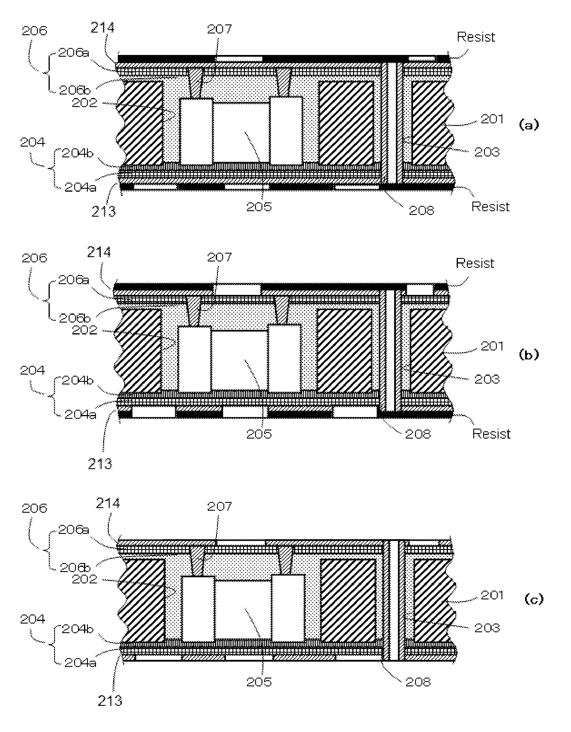
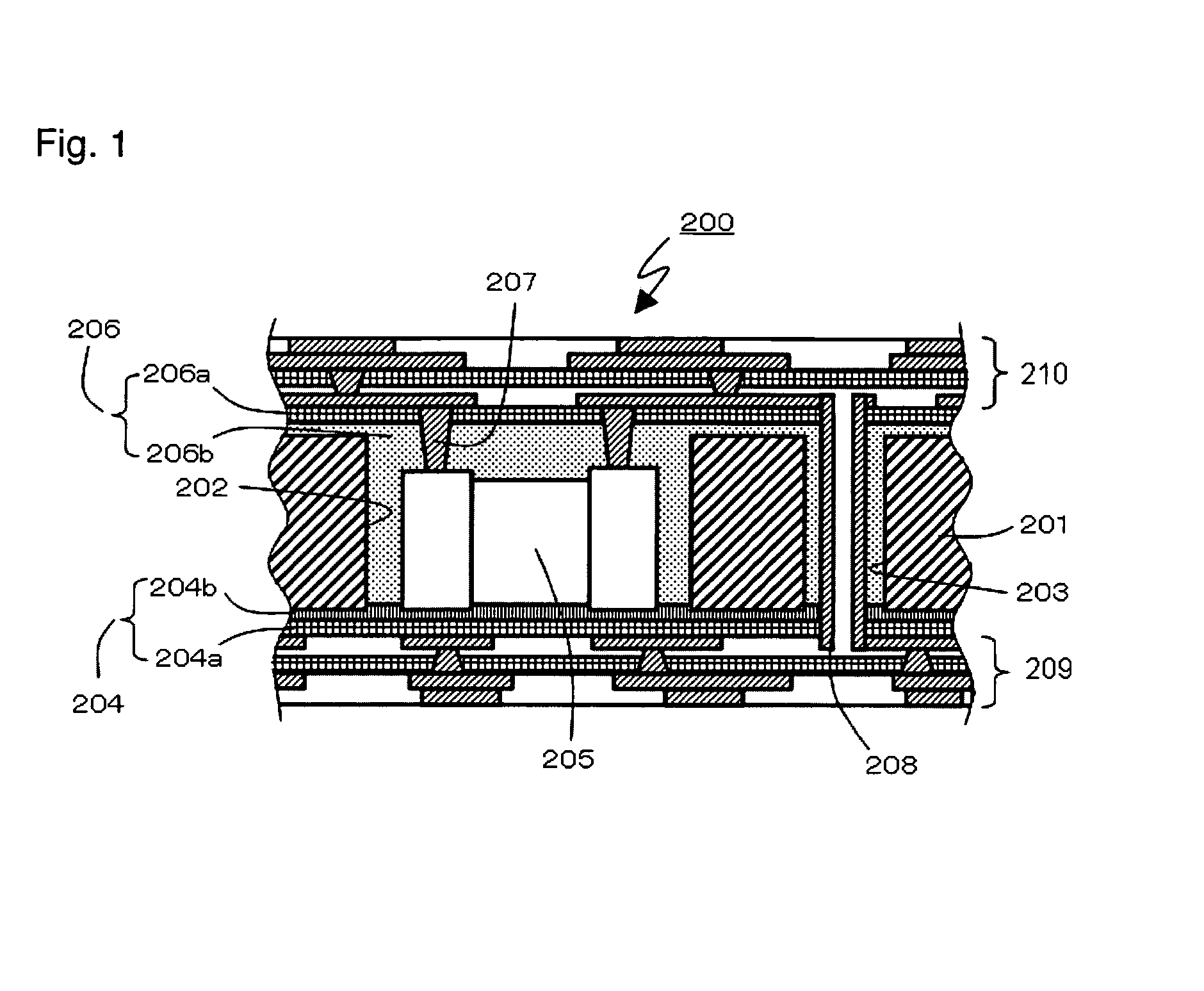
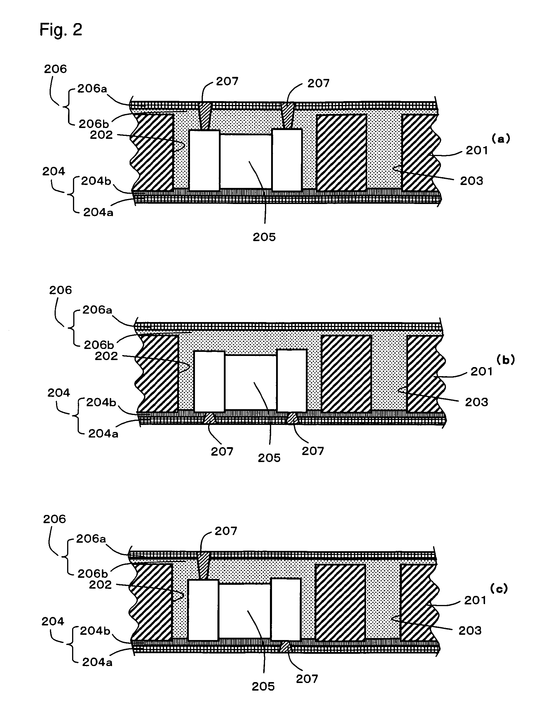
[0096]FIG. 1 is an illustration showing a structure of an electronic part-incorporated multilayer substrate according to an embodiment of the invention. The embodiment described below is an electronic part-incorporated multilayer substrate and employing a core formed from a metal or an organic material. Referring to FIG. 1, a multi-layer substrate 200 includes a core 201 formed with a hole 202 in which an electronic part can be contained and a through hole 203 which is to serve to form a through hole 208. A bottom insulating resin layer 204 is formed on one side of the core, and a top insula...


PUM

PropertyMeasurementUnit
thicknessaaaaaaaaaa
thicknessaaaaaaaaaa
thicknessaaaaaaaaaa

Abstract

In a multi-layer substrate including a core formed with a plurality of holes capable of containing an electronic part, a bottom insulating resin layer formed on a bottom surface of the core, a top insulating resin layer formed on a top surface of the core, a wiring layer selectively formed on an outer layer of the bottom insulating resin layer or top insulating resin layer, and an electronic part contained in the holes, both of the bottom and top insulating resin layers have a structure that is a combination of a resin which is changed to cohesiveness when heated and which undergoes smaller plastic deformation when heated to a higher temperature and an insulating resin layer which has a thickness sufficient to maintain insulation between the electronic part or a conductor of the core and the wiring layer and which inherently undergoes small plastic deformation, so that the electronic part can be securely and sealed in the holes without using a particular adhesive.

Description

BACKGROUND OF THE INVENTION[0001]1. Field of the Invention[0002]The present invention relates to an electronic part-incorporated multilayer substrate and a method of producing the same. More particularly, the invention relates to an electronic part-incorporated multilayer substrate having a structure in which a core made of a metal or an organic material and formed with an electronic part accommodation part is sealed with an insulating resin layer. The invention also relates to a method of producing such a multi-layer substrate.[0003]2. Description of the Related Art[0004]As a result of the diversification of portable equipment, an electronic part-incorporated multilayer substrate having a structure as described above have come into use as functional modules, semiconductor packages, and mother boards for various applications including cellular phone, portable electronic dictionaries, personal information instruments (sometime abbreviated as PDAs), and digital cameras (sometimes abbr...

Claims


Application Information

Patent Timeline
Patent Type & Authority Patents(United States)
IPC IPC(8): H05K1/18H05K3/30
CPCH05K1/185H05K1/056H05K3/445H05K3/4608H05K3/4661H05K2201/0195Y10T29/49155H05K2201/10636H05K2203/1152H05K2203/1469Y10T29/4913Y10T29/49124Y10T29/49126H05K2201/0209H01L24/24H01L24/82H01L2224/04105H01L2224/2518H01L2224/73267H01L2224/92244H01L2924/14H01L2924/3025H01L2924/351Y02P70/50H01L2924/00
Inventor INOUE, YUSUKEMUGIYA, EIJIMIYAZAKI, MASASHISAWATARI, TATSUROSUGIYAMA, YUICHI
Owner TAIYO YUDEN KK
Why Eureka
Try Eureka