Memory cell, a memory array and a method of programming a memory cell

a memory cell and array technology, applied in the field of memory cells, can solve the problems of insufficient data retention of sonos memory cells, inability to increase the thickness of the bottom silicon oxide of a sonos transistor above approximately 2.5 nanometers (nm), and achieve the effect of fast and efficient mass erasure of a complete memory produ

Inactive Publication Date: 2012-11-27
NXP BV
View PDF17 Cites 6 Cited by
  • Summary
  • Abstract
  • Description
  • Claims
  • Application Information

AI Technical Summary

Benefits of technology

[0026]According to an exemplary embodiment of the invention, a scheme of programming a memory cell may be provided. Firstly, charge carriers (for instance electrons) are accelerated by applying a first voltage to a dedicated terminal, particularly between two source / drain regions of a memory transistor. When a suitable second electrical potential is then applied to another dedicated terminal, particularly the gate terminal of the memory transistor, second charge carriers (for instance holes) generated by impact ionisation may tunnel even through a relatively thick silicon oxide layer into a charge trapping structure such as a silicon nitride layer of an ONO (silicon oxide-silicon nitride-silicon oxide) layer sequence. Information to be stored in such a memory cell may be encoded in the presence or absence, in the amount and / or in the charge type of the electrically charged particles trapped in the charge trapping layer. This information may be read out by applying a sampling voltage to the memory transistor (and / or by applying a sampling voltage to an access transistor), and the amount of the flowing current (between source and drain) then depends on the previous programming scheme. Since the hot hole injection procedure triggered by impact ionisation allows the use of a thick gate insulating layer of the memory transistor, the data retention time may be significantly increased using embodiments of the invention.
[0056]A plurality of memory cells of a memory array (for instance all memory cells of a memory array) may be erased simultaneously. This may allow for a fast and efficient mass erasure of a complete memory product.

Problems solved by technology

However, data retention of SONOS memory cells may be insufficiently small.
However, when implementing direct tunneling processes, the bottom silicon oxide thickness of a SONOS transistor cannot be increased above approximately 2.5 nanometer (nm) to improve the data retention time because the hole tunneling from the substrate to the silicon nitride during erasing may become extremely low and the erasing may become inefficient.
As may be taken from FIG. 3, erase is simply not possible.
From FIG. 2 and FIG. 3, it may be taken that it may be very difficult to improve the retention time of a SONOS device operated by tunneling procedures.
However, the retention time of a memory arrangement according to US 2004 / 0155234 A1 may be insufficient.

Method used


Image

  • Memory cell, a memory array and a method of programming a memory cell
  • Memory cell, a memory array and a method of programming a memory cell
  • Memory cell, a memory array and a method of programming a memory cell

Examples


Embodiment Construction

[0078]The illustration in the drawing is schematical. In different drawings, similar or identical elements are provided with the same reference signs.

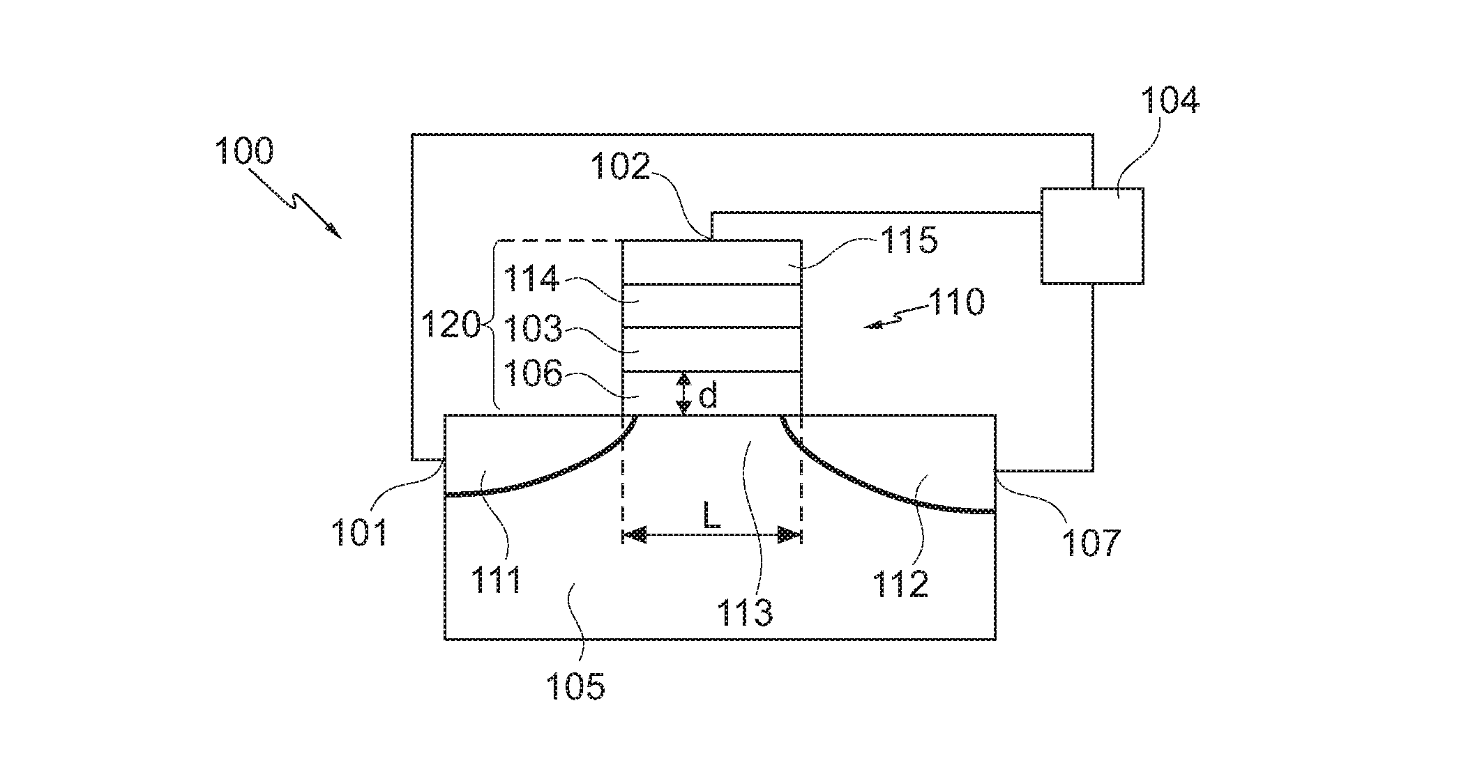
[0079]In the following, referring to FIG. 1, a memory cell 100 according to an exemplary embodiment of the invention will be explained.

[0080]The memory cell 100 comprises a first electric terminal 101 serving as a first source- / drain terminal, a second electrical terminal 102 serving as a gate terminal, a charge trapping structure 103 configured as a silicon nitride layer and a programming unit 104. The programming unit 104 may be an integrated circuit or may be a voltage control device provided externally of s silicon substrate 105 of the memory cell. The programming unit 104 is adapted for applying a first electric potential to the first electric terminal 101 to accelerate electrons in a channel region 113 to thereby generate positively charged holes by impact ionisation of the accelerated electrons in the substrate 105. The programm...


PUM


Abstract

A method of programming a memory cell (100), the method comprising applying a first electric potential to a first electric terminal (101) of the memory cell (100) to accelerate first charge carriers of a first type of conductivity to thereby generate second charge carriers of a second type of conductivity by impact ionisation of the accelerated first charge carriers, and applying a second electric potential to a second electric terminal (102) of the memory cell (100) to accelerate the second charge carriers to thereby inject the second charge carriers in a charge trapping structure (103) of the memory cell (100).

Description

FIELD OF THE INVENTION[0001]The invention relates to a memory cell.[0002]Moreover, the invention relates to a memory array.[0003]Beyond this, the invention relates to a method of programming a memory cell.BACKGROUND OF THE INVENTION[0004]The storage of information on computer systems and in embedded chips for smartcards, etc. becomes more and more important. Particularly, flash memory arrays may be employed for this purpose.[0005]SONOS (silicon-silicon oxide-silicon nitride-silicon oxide-silicon) and charge trapping memories in general (for instance nanocrystals, SONOS with one or more layers made of a high k-material, etc.) are serious candidates for embedded and stand alone non-volatile memories in the 45 nm CMOS generation and beyond, thanks to the ease of integration in the CMOS flow and the low program and erase voltages compared to floating gate devices.[0006]However, data retention of SONOS memory cells may be insufficiently small. In fact, SONOS cells are operated by direct ...

Claims


Application Information

Patent Timeline
Patent Type & Authority Patents(United States)
IPC IPC(8): G11C11/34
CPCG11C16/0466G11C16/0433
Inventor AKIL, NADERVAN DUUREN, MICHIEL
Owner NXP BV
Why Eureka
Try Eureka