Eureka AIR delivers breakthrough ideas for toughest innovation challenges, trusted by R&D personnel around the world.

Pinning field in MR devices despite higher annealing temperature

a technology of magnetoresistive devices and mr, which is applied in the field of magnetoresistive devices, can solve the problems that the ru7.5 system cannot produce sufficient hs, and achieve the effect of high internal pinning strength and high mr ratio

Active Publication Date: 2012-12-04
HEADWAY TECH INC
View PDF10 Cites 5 Cited by
  • Summary
  • Abstract
  • Description
  • Claims
  • Application Information

AI Technical Summary

Benefits of technology

[0010]It has been an object of at least one embodiment of the present invention to provide a method for combining both a high internal pinning strength and a high MR ratio in the same MR device.
[0013]A further object of at least one embodiment of the present invention has been to reduce the thickness of such a TMR device in order to improve pattern resolution.
[0014]These objects have been achieved by reducing interfacial roughness of the ruthenium layer located between AP1 and AP2, by minimizing boron diffusion from AP1 into the ruthenium, and by minimizing manganese diffusion from the AFM layer into the ruthenium layer.
[0015]Specifically, a plasma treatment after AFM deposition, but before Ru deposition, has been added to the manufacturing process to reduce the development of interfacial roughness during Ru layer growth. Additionally, a thin CoFex layer is laid down immediately after Ru deposition to block boron diffusion from the AP1 layer:

Problems solved by technology

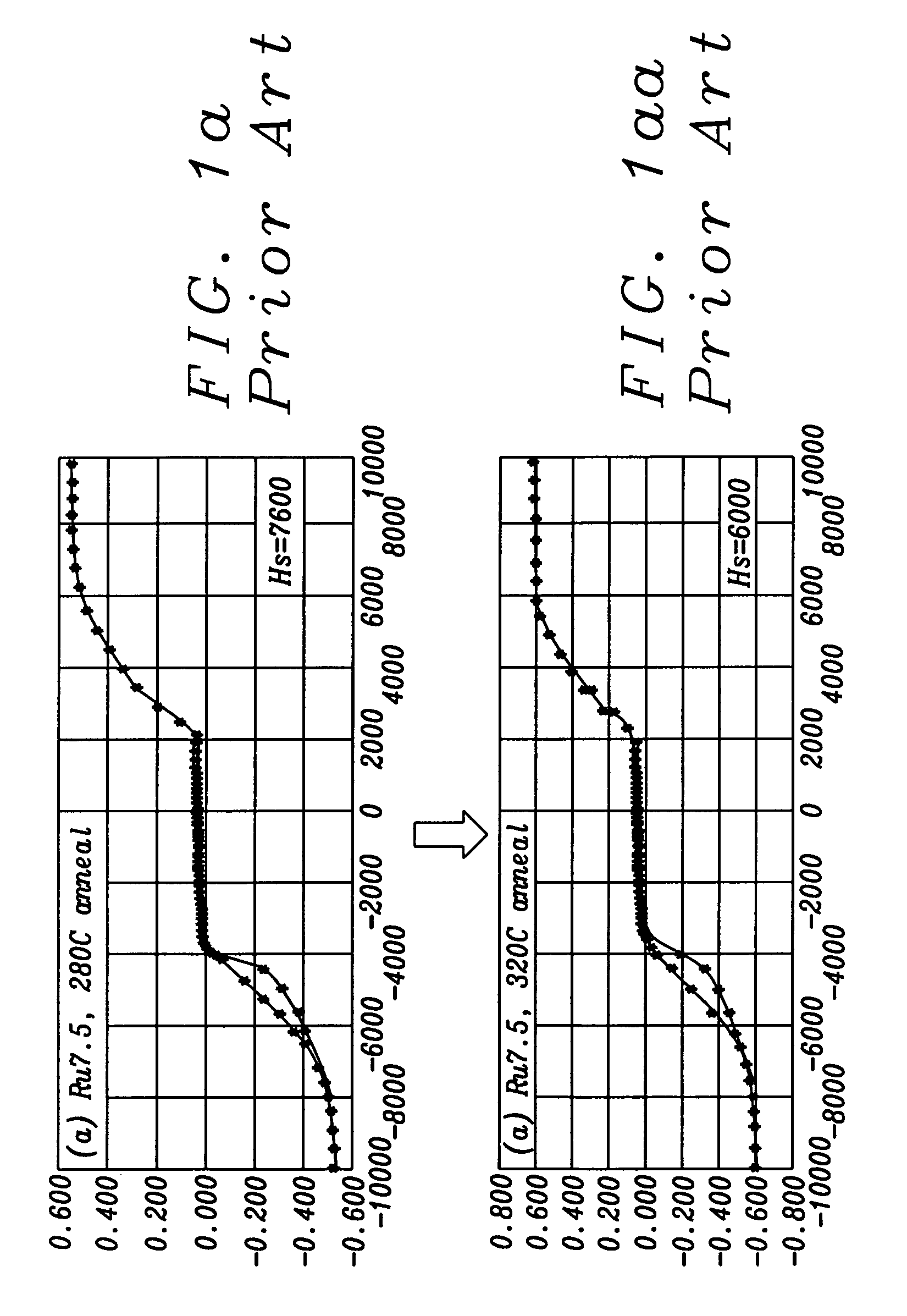
Thus, at some point, SyAP with Ru7.5 will no longer be capable of producing sufficient Hs.

Method used


Image

  • Pinning field in MR devices despite higher annealing temperature
  • Pinning field in MR devices despite higher annealing temperature
  • Pinning field in MR devices despite higher annealing temperature

Examples


Embodiment Construction

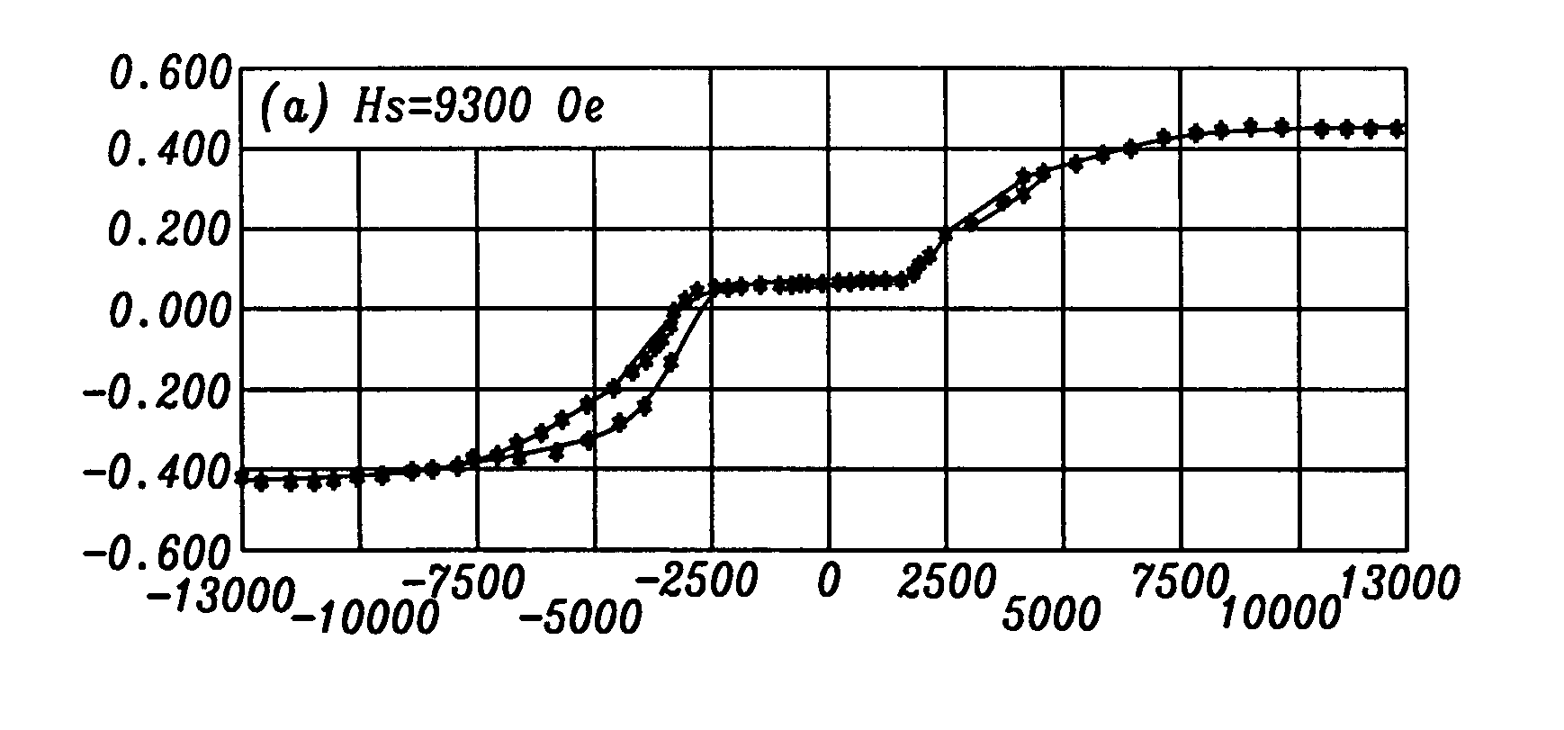
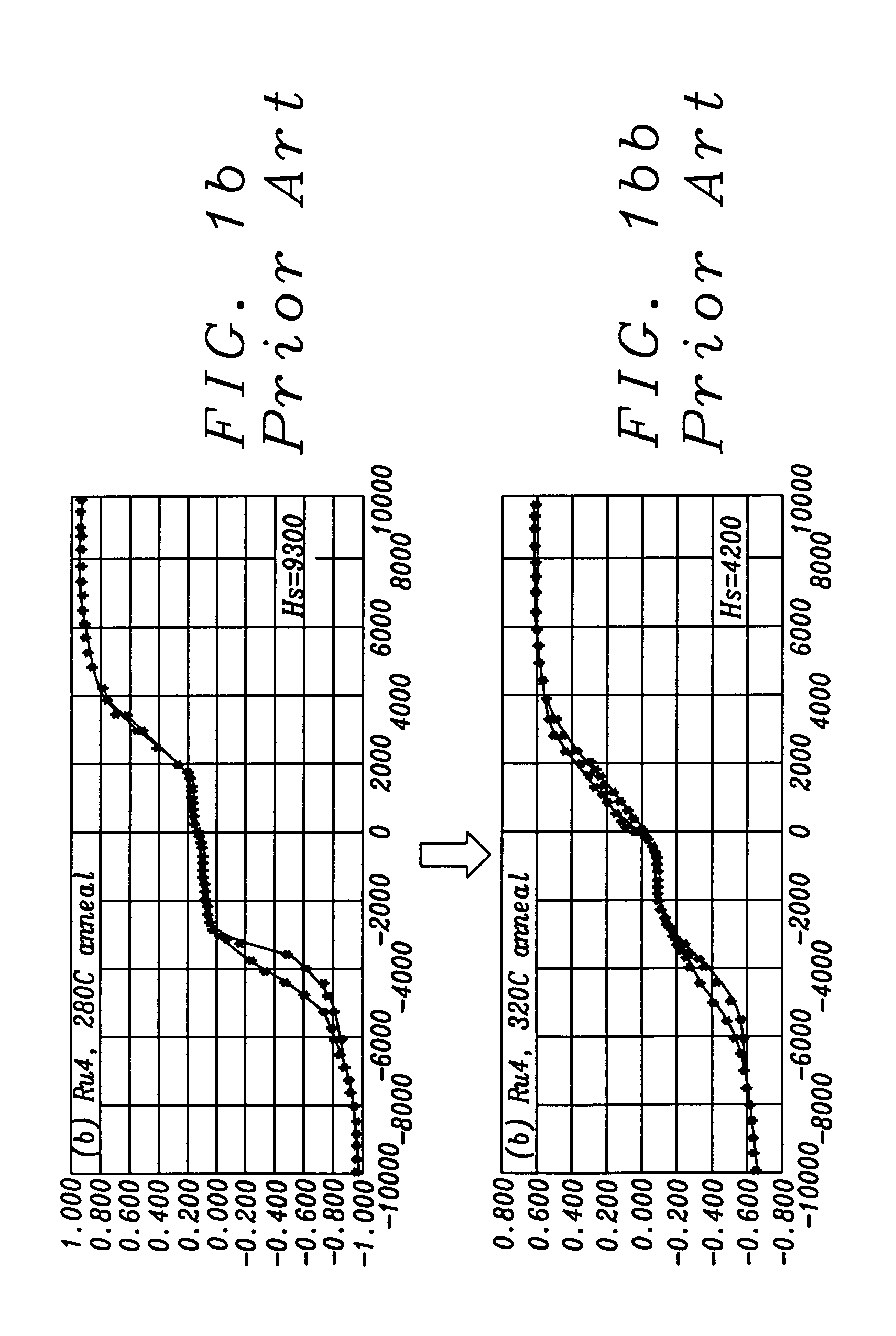
[0021]The invention discloses how, using an improved SyAP based on the Ru first peak (Ru 4A), ensures a high Hs for a TMR sensor, thereby enabling a higher annealing temperature to be used with said TMR sensor which in turn leads to a higher MR ratio.

[0022]As noted earlier, SyAP with a Ru first peak at Ru4A has, intrinsically, a much greater Hs field than with a Ru second peak at Ru7.5A. Therefore, in order to retain the pinning strength needed to ensure good device performance after exposure to the higher annealing temperature, we have to improve the pinning properties of Ru4A SyAP systems.

[0023]In order to accomplish this, we need to eliminate, or greatly reduce, the Hs degradation that occurs at higher annealing temperature. We have determined that this Hs degradation is due to the following factors:

[0024]1) increased Ru interfacial roughness due to grain growth at the higher annealing temperature;

[0025]2) boron diffusion from the AP1 CoFeB material into the Ru interface; and

[002...


PUM

PropertyMeasurementUnit
thicknessaaaaaaaaaa
thicknessaaaaaaaaaa
temperatureaaaaaaaaaa

Abstract

The pinning field in an MR device was significantly improved by using the Ru 4A peak together with steps to minimize interfacial roughness of the ruthenium layer as well as boron and manganese diffusion into the ruthenium layer during manufacturing. This made it possible to anneal at temperatures as high as 340° C. whereby a high MR ratio could be simultaneously achieved.

Description

FIELD OF THE INVENTION[0001]The invention relates to the general field of magneto-resistive devices with particular attention the simultaneous improvement of both the MR ratio and the pinning strength of the SyAP portion of the device.BACKGROUND OF THE INVENTION[0002]RKKY (Ruderman-Kittel-Kasuya-Yosida) coupling is a particular type of magnetic coupling due to interaction between the conduction electrons, making possible the creation, and widespread use of, synthetic AntiParallel (SyAP) structures (AP2 / Ru / AP1). For MgO barrier based tunneling magneto-resistive (TMR) sensors, a typical structure would comprise:[0003]Seed / antiferromagnetic (AFM) layer / AP2 / Ru / AP1 / MgOx / free layer / capping layer.[0004]A ruthenium thickness of 7.5 Angstroms (Ru7.5) is commonly used in the AP2 / Ru / AP1 portion because it is easy to control and is not too sensitive to Ru interfacial condition changes. However, as device and film stack size become ever smaller, the pinning field, which is limited by the saturat...

Claims


Application Information

Patent Timeline
Patent Type & Authority Patents(United States)
IPC IPC(8): G11B5/127
CPCH01L43/08H01L43/12B82Y40/00H01F41/307H01F10/3259H01F10/3272H01L29/82H10N50/01H10N50/10
Inventor ZHANG, KUNLIANGWANG, SHENGYUANZHAO, TONGLI, MINWANG, HUI-CHUAN
Owner HEADWAY TECH INC
Why Eureka
Eureka Blog
Learn More