Organic light-emitting device

a light-emitting device and organic technology, applied in the direction of thermoelectric device junction materials, semiconductor devices, electrical apparatus, etc., can solve the problems of reducing the luminous efficiency of each of the devices, the inability to achieve sufficient luminous efficiency for practical use, and the long life of phosphorescence emitted from each of the light-emitting materials, etc., to achieve high luminous efficiency

Inactive Publication Date: 2012-12-11
CANON KK
View PDF28 Cites 13 Cited by
  • Summary
  • Abstract
  • Description
  • Claims
  • Application Information

AI Technical Summary

Benefits of technology

[0014]An object of the present invention is to provide an organic light-emitting device that shows high luminous efficiency even when driven at a high luminance.
[0016]According to the present invention, it is possible to provide an organic light-emitting device that shows high luminous efficiency even when driven at a high luminance.

Problems solved by technology

However, luminous efficiency sufficient for practical use has not been realized at present.
Meanwhile, in the case of the organic light-emitting devices using the phosphorescent light-emitting materials, the lifetime of phosphorescence emitted from each of the light-emitting materials is long.
As a result, a ratio of the amount of triplet excitons each of which is deactivated (emits light) to the amount of excitons produced per unit time increases, and hence the luminous efficiency of each of the devices reduces.
Each of the devices has high luminous efficiency in a low-luminance region but cannot utilize the high luminous efficiency in a high-luminance region, and as a result, its power consumption increases.
In addition, excitons produced by the recombination of holes and electrons disappear owing to the formation of the charge transfer complex or exciplex, and as a result, luminous efficiency may reduce.
In addition, an additional investigation on the case where a high current is flowed is needed because a carrier balance may be lost and the luminous efficiency may reduce in the case.
In addition, when a phosphorescent light-emitting dopant whose luminescent color is green or blue is used, the number of kinds of materials capable of being responsible for intersystem crossing each of which is to be used as the second dopant is small, and hence it has been difficult to optimize a combination of the dopants.

Method used


Image

  • Organic light-emitting device
  • Organic light-emitting device
  • Organic light-emitting device

Examples


example 1

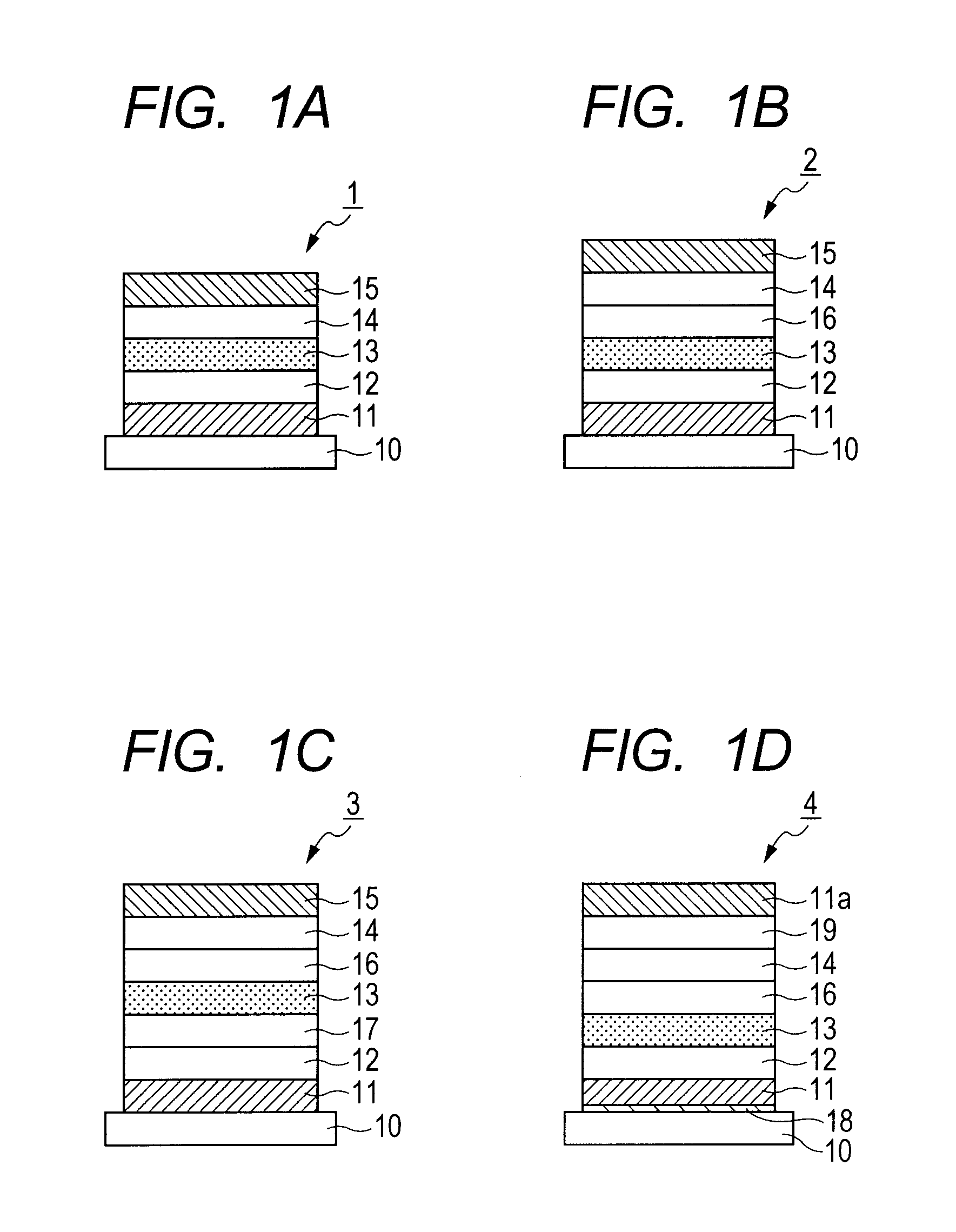
[0098]An organic light-emitting device having the configuration illustrated in FIG. 1A was produced. First, an ITO was formed into a film on a glass substrate (the transparent substrate 10) by a sputtering method. Thus, the transparent electrode 11 (anode) was formed. In this case, the thickness of the transparent electrode 11 was set to 100 nm. Next, patterning was performed by a photolithography step so that the transparent electrode had an area of 3.14 mm2. Next, organic compound layers and electrode layers shown in Table 2 below were continuously formed in the order on the substrate on which the ITO film had been formed by performing vacuum deposition based on resistance heating in a vacuum chamber at 1×10⁻⁴ Pa.

[0099]

TABLE 2Organic compound layers andThicknesselectrode layersConstituents[nm]Hole transport layer 12Compound A240Emission layer 13H1 (host)50D1 (first dopant)A3 (seconddopant)(H1:D1:A3 =80:4:16 (weightratio)Electron transport layer 14ET225MetalFirst metalKF1electrodee...

example 2

[0113]An organic light-emitting device having the configuration illustrated in FIG. 1B was produced. First, an ITO was formed into a film on a glass substrate (the transparent substrate 10) by a sputtering method. Thus, the transparent electrode 11 (anode) was formed. In this case, the thickness of the transparent electrode 11 was set to 100 nm. Next, patterning was performed by a photolithography step so that the transparent electrode had an area of 3.14 mm2. Next, organic compound layers and electrode layers shown in Table 3 below were continuously formed in the order on the substrate on which the ITO film had been formed by performing vacuum deposition based on resistance heating in a vacuum chamber at 1×10⁻⁴ Pa.

[0114]

TABLE 3Organic compound layersThicknessand electrode layersConstituents[nm]Hole transport layer 12Compound A240Emission layer 13H2 (host)50D1 (first dopant)A2 (second dopant)(H2:D1:A2 =80:4:16 (weightratio))Hole / exciton-blockingET110layer 16Electron transport layerE...

example 3

[0117]An organic light-emitting device was produced in the same manner as in Example 1 except that Compound A1 was used instead of Compound A2 as the second dopant in Example 2.

[0118]An emission spectrum was measured in the same manner as in Example 1. As a result, an emission spectrum mainly derived from Compound D1 as a light-emitting dopant was observed. In addition, the device was evaluated for its light-emitting property in the same manner as in Example 1. Table 4 shows the result.


PUM


Abstract

Provided is an organic light-emitting device that shows high luminous efficiency even when driven at a high luminance. More specifically, provided is an organic light-emitting device, including: an anode (transparent electrode layer) and a cathode (metal electrode layer); and an organic compound layer being interposed between the anode and the cathode, and including an emission layer, in which: the emission layer has a host, a first dopant, and a second dopant; the host includes an aromatic hydrocarbon compound; the first dopant includes a phosphorescent iridium complex; and the second dopant includes a compound having two triarylamine structures.

Description

BACKGROUND OF THE INVENTION[0001]1. Field of the Invention[0002]The present invention relates to an organic light-emitting device.[0003]2. Description of the Related Art[0004]Investigations have been vigorously conducted on organic light-emitting devices as flat light sources and as components for thin display panels at present. The organic light-emitting devices are each an electron device formed of: two electrodes; and a multilayer thin film formed of organic amorphous charge transport materials interposed between the two electrodes. In addition, the organic light-emitting devices are each such an electron device that charges (holes and electrons) are injected from the electrodes toward the thin film, the charges recombine in a specific compound to excite the specific compound, and light emitted in the deactivation process of the excited compound is extracted. Reports on the organic light-emitting devices available since olden times are, for example, light emission by the applicat...

Claims


Application Information

Patent Timeline
Patent Type & Authority Patents(United States)
IPC IPC(8): H01L51/52H01L51/54
CPCH01L51/5016H01L51/0085H10K85/342H10K50/11H10K2101/10
Inventor OOISHI, RYOTAKAMATANI, JUNKISHINO, KENGOKOSUGE, TETSUYAABE, SHIGEMOTO
Owner CANON KK
Why Eureka
Try Eureka