

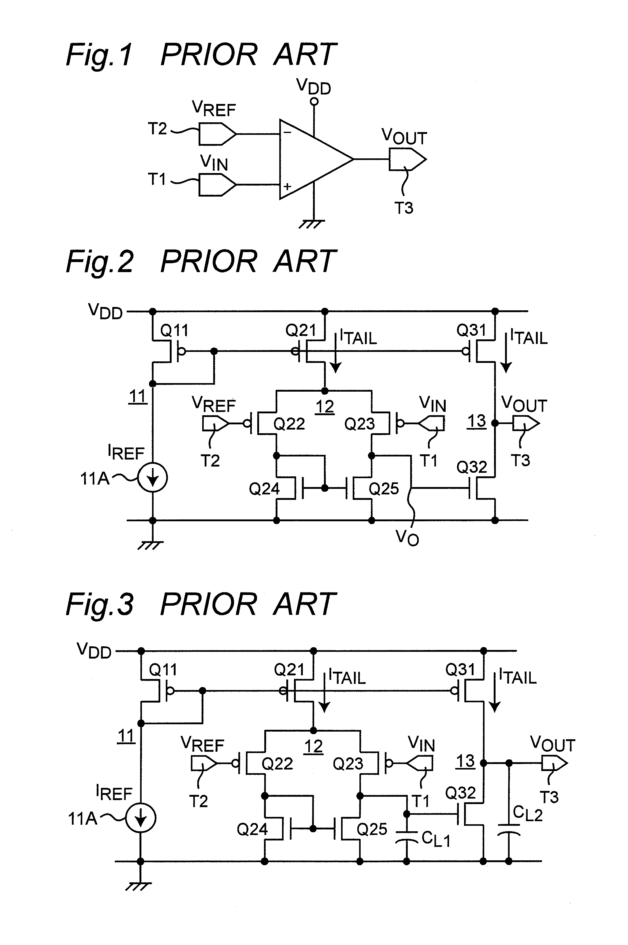
Comparator circuit provided with differential amplifier making logical judgment by comparing input voltage with reference voltage
a technology of differential amplifier and comparator circuit, which is applied in the direction of pulse circuit, pulse technique, instant pulse delivery arrangement, etc., can solve the problems of simple voltage gain, reduce the logical judgment time of signal processing, increase the adaptive bias current, and improve the speed
- Summary
- Abstract
- Description
- Claims
- Application Information
AI Technical Summary
Benefits of technology
Problems solved by technology
Method used
Image

Examples
first preferred embodiment
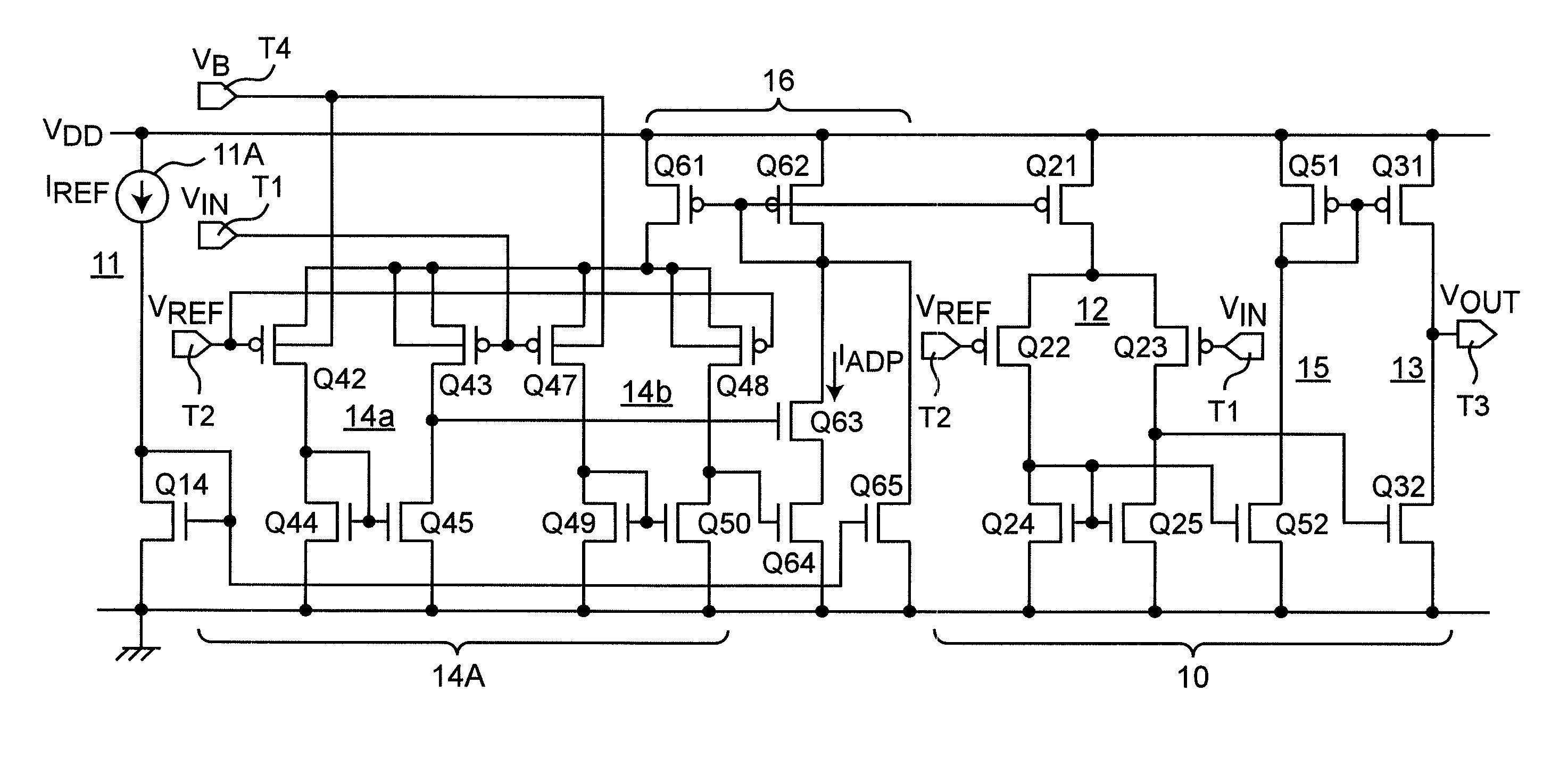
[0079]FIG. 7 is a circuit diagram showing a configuration of an adaptive bias current control system comparator circuit utilizing a body bias effect according to the first preferred embodiment of the invention. The aforementioned comparator circuit of NPS Inc. (FIG. 5) operates in a subthreshold region. Therefore, the technique for generating an offset voltage by the size ratio of the differential pair configured to include the two differential amplifiers 14a and 14b and the size ratio of the current mirror circuits has had such a problem that the size ratio, which is contained in the logarithmic term, produces small effects appearing as an offset voltage and only a minute offset voltage can be generated.
[0080]In the first preferred embodiment of the invention, a technique for more effectively generating the offset voltage was estimated. The idea of utilizing the two differential amplifiers 14a and 14b is identical to the technique of the comparator circuit of FIG. 5. However, in co...
second preferred embodiment
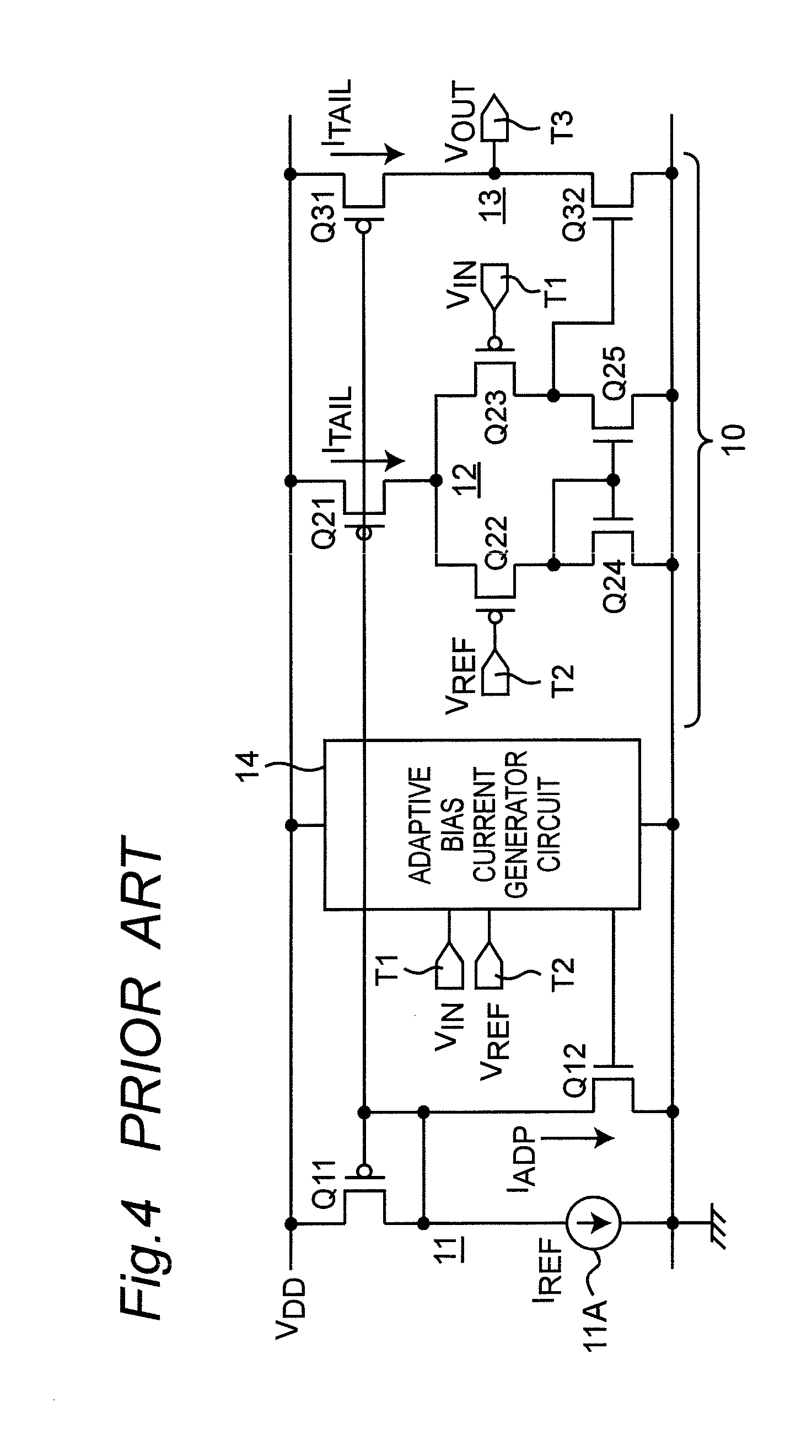
[0083]FIG. 9A is a circuit diagram showing a configuration of an adaptive bias current control system comparator circuit that utilizes the through current ISC of a CMOS inverter circuit according to the second preferred embodiment of the invention. In the configuration of the comparator circuit proposed by the first preferred embodiment and its modified preferred embodiment, two differential amplifiers 14a and 14b are required for the adaptive bias current generator circuit 14. For the above reasons, there is such a problem that the mounting scale of the circuit is relatively large. Accordingly, a circuit configuration capable of remarkably reducing the circuit scale was estimated. It is noted that the through current ISC of the CMOS inverter circuit is defined as a current that flows when the MOSFETs are both turned on.
[0084]FIG. 9A is characterized by including such a circuit configuration that the output voltage of the differential amplifier 12 is monitored by an inverter circuit...
third preferred embodiment
[0091]FIG. 11 is a circuit diagram showing a configuration of a comparator circuit according to the third preferred embodiment of the invention, in which the leak current of the inverter 13 of the final stage is reduced to solve the problem of the comparator circuit of FIG. 10. In order to solve the problem of the comparator circuit of FIG. 10, the circuit is characterized by including an adaptive bias current generator circuit 19B, in which a generator circuit of the minute bias current IREF and a generator circuit of the adaptive bias current IADP of the through current ISC are configured to include separate current mirror circuits.
[0092]In the differential amplifier 12A of FIG. 11, the bias current IREF is applied as a bias to the differential amplifier 12A via a current mirror circuit configured to include MOSFETs Q11 and Q21a. Likewise, the adaptive bias current IADP of the through current ISC of the inverter circuit 17 is applied as a bias to the differential amplifier 12 via ...
PUM
 Abstract
Description
Claims
Application Information