Semiconductor device

a technology of semiconductors and semiconductors, applied in the direction of digital storage, capacitors, instruments, etc., can solve the problems of extremely low leakage current of transistors including highly purified oxide semiconductors, data can be stored for a long time, etc., to achieve the effect of reducing power consumption, storing data for an extremely long time, and avoiding the frequency of refresh operation

Active Publication Date: 2012-12-25
SEMICON ENERGY LAB CO LTD
View PDF155 Cites 25 Cited by
  • Summary
  • Abstract
  • Description
  • Claims
  • Application Information

AI Technical Summary

Benefits of technology

[0011]In the disclosed invention, a semiconductor device is formed using a highly-purified oxide semiconductor. The leakage current of a transistor including a highly-purified oxide semiconductor is extremely low, whereby data can be stored for a long time.
[0026]Since the off-state current of a transistor including an oxide semiconductor is extremely low, stored data can be stored for an extremely long time with the use of the transistor. In other words, power consumption can be adequately reduced because refresh operation becomes unnecessary or the frequency of refresh operation can be extremely low. Moreover, stored data can be stored for a long time even when power is not supplied.
[0027]Further, in a semiconductor device of the disclosed invention, high voltage is not needed to write data, and deterioration of the element does not become a problem. For example, there is no need to perform injection of electrons to a floating gate and extraction of electrons from the floating gate which are needed in a conventional nonvolatile memory; therefore, deterioration of a gate insulating layer does not occur. In other words, the semiconductor device of the disclosed invention does not have a limit on the number of times of writing operations, which is a problem in a conventional nonvolatile memory, and reliability thereof is drastically improved. Further, data is written by switching an on state and an off state of the transistor, whereby high-speed operation can be easily realized. In addition, there is no need of operation for erasing data.
[0028]In addition, because a transistor including a material other than an oxide semiconductor can sufficiently operate at high speed, operation speed of a semiconductor device (e.g., data read operation) can be sufficiently high by combining the transistor including a material other than an oxide semiconductor with a transistor including an oxide semiconductor. Further, a transistor including a material other than an oxide semiconductor makes it possible to realize circuits that need to operate at high speed (e.g., a logic circuit and a driver circuit) preferably.

Problems solved by technology

The leakage current of a transistor including a highly-purified oxide semiconductor is extremely low, whereby data can be stored for a long time.

Method used


Image

  • Semiconductor device
  • Semiconductor device
  • Semiconductor device

Examples


embodiment 1

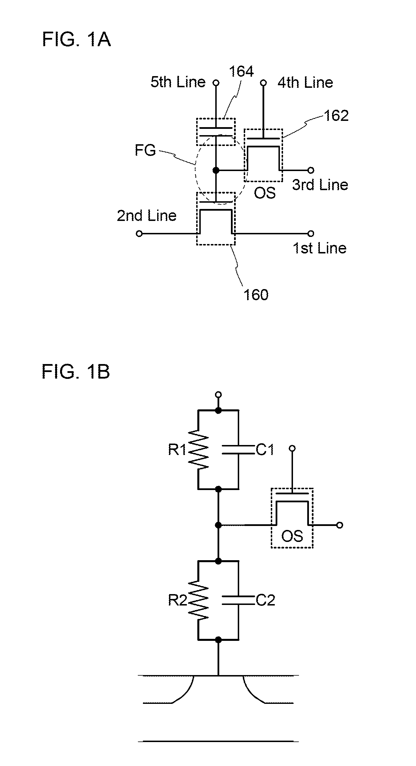
[0053]In Embodiment 1, a circuit structure and operation of a semiconductor device of one embodiment of the disclosed invention will be described with reference to FIGS. 1A and 1B. Note that in some circuit structures, “OS” is written beside a transistor in order to indicate that the transistor includes an oxide semiconductor.

[0054]In a semiconductor device in FIG. 1A, a first wiring (which is denoted by “1st Line” and also referred to as a source line SL) and a source electrode of a transistor 160 are electrically connected to each other, and a second wiring (which is denoted by “2nd Line” and also referred to as a bit line BL) and a drain electrode of the transistor 160 are electrically connected to each other. A gate electrode of the transistor 160 and one of a source and drain electrodes of the transistor 162 are electrically connected to one of electrodes of a capacitor 164. A third wiring (which is denoted by “3rd Line” and also referred to as a first signal line S1) and the o...

embodiment 2

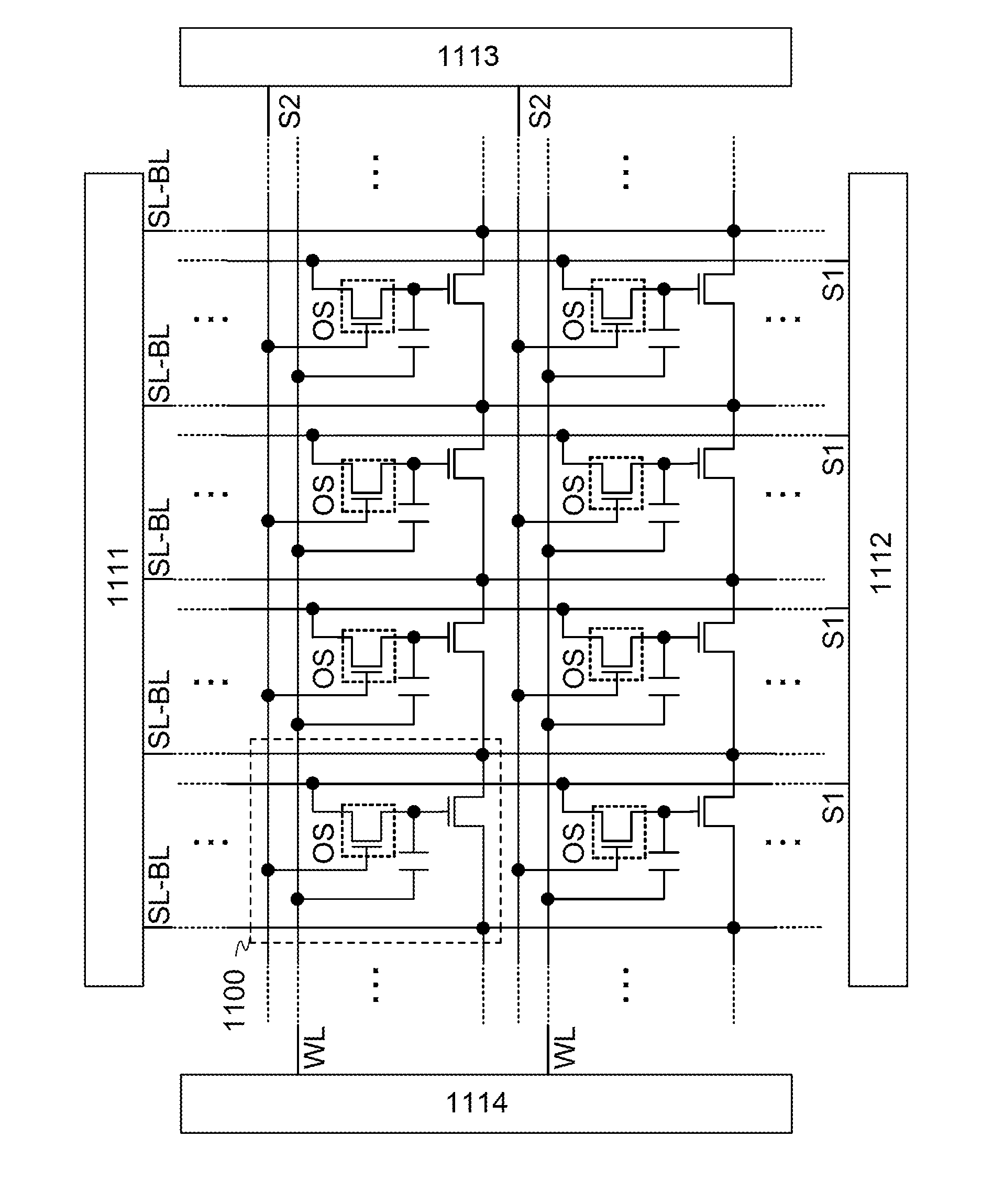
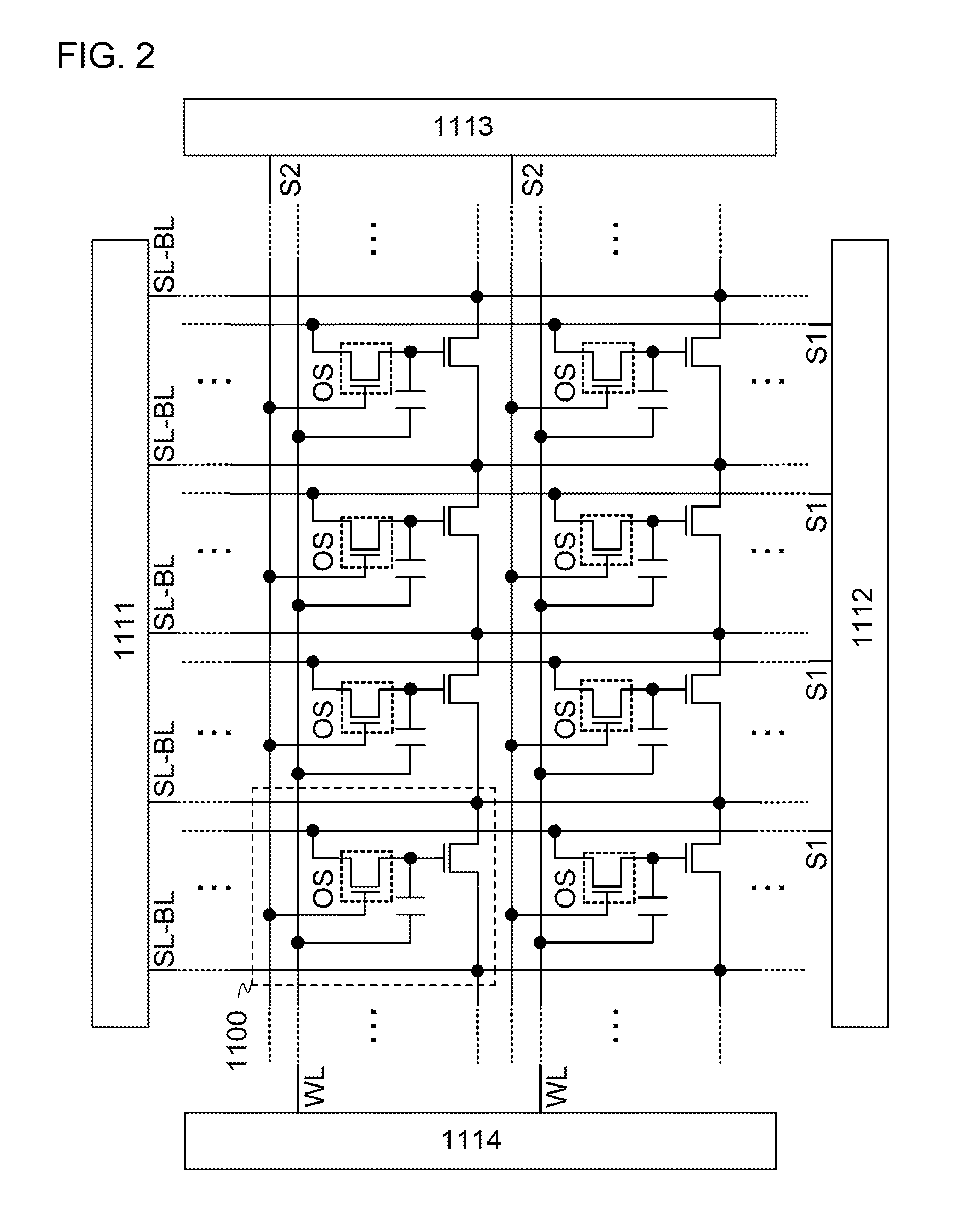
[0090]In Embodiment 2, one application example of the semiconductor device described in Embodiment 1 will be explained. Specifically, one example of a semiconductor device in which the semiconductor devices described in Embodiment 1 are arranged in matrix will be explained.

[0091]FIG. 2 illustrates one example of a circuit diagram of a semiconductor device having storage capacity of m×n bits.

[0092]The semiconductor device of one embodiment of the present invention includes m word lines WL, m second signal lines S2, (n+1) source-bit lines SL-BL, n first signal lines S1, a memory cell array where a plurality of memory cells 1100 are arranged in matrix of m (rows) (in a vertical direction)×n (columns) (in a horizontal direction) (m and n are natural numbers), and peripheral circuits such as a first driver circuit 1111, a second driver circuit 1112, a third driver circuit 1113, and a fourth driver circuit 1114. Here, the structure described in the foregoing embodiment (e.g., the structur...

embodiment 3

[0133]In Embodiment 3, another example of a semiconductor device in which the semiconductor devices described in Embodiment 1 are arranged in matrix will be explained. Hereinafter, portions different from those in the foregoing embodiments will be described and a detailed description of portions similar to those in the foregoing embodiments is omitted.

[0134]FIG. 5 illustrates one example of a circuit diagram of a semiconductor device having storage capacity of m×n bits. In Embodiment 3, unlike Embodiment 2, an example will be described in which the second signal lines S2 are provided so as to be extended in a column direction and the first signal lines S1 are provided so as to be extended in a row direction.

[0135]The semiconductor device of one embodiment of the present invention includes m word lines WL, m first signal lines S1, (n+1) source-bit lines SL-BL, n second signal lines S2, a memory cell array where a plurality of memory cells 1200 are arranged in matrix of in (rows) (in ...


PUM


Abstract

An object is to provide a semiconductor device with a novel structure in which stored data can be retained even when power is not supplied, and does not have a limitation on the number of times of writing operations. A semiconductor device includes a source-bit line, a first signal line, a second signal line, a word line, and a memory cell connected between the source-bit lines. The memory cell includes a first transistor, a second transistor, and a capacitor. The second transistor is formed including an oxide semiconductor material. A gate electrode of the first transistor, one of a source and drain electrodes, and one of electrodes of the capacitor are electrically connected to one another. The source-bit line and a source electrode of the first transistor are electrically connected to each other. Another source-bit line adjacent to the above source-bit line and a drain electrode of the first transistor are electrically connected to each other.

Description

TECHNICAL FIELD[0001]The invention disclosed herein relates to a semiconductor device using a semiconductor element and a method for manufacturing the semiconductor device.BACKGROUND ART[0002]Storage devices using semiconductor elements are broadly classified into two categories: a volatile memory device that loses stored data when power supply stops, and a non-volatile memory device that retains stored data even when power is not supplied.[0003]A typical example of a volatile storage device is a DRAM (dynamic random access memory). A DRAM stores data in such a manner that a transistor included in a storage element is selected and charge is stored in a capacitor.[0004]When data is read from a DRAM, charge in a capacitor is lost on the above-described principle; thus, another writing operation is needed when data is stored again after data is read. A data storage period is short because charge flows from / into a transistor forming a memory element by leakage current between a source a...

Claims


Application Information

Patent Timeline
Patent Type & Authority Patents(United States)
IPC IPC(8): G11C11/24G11C11/22
CPCG11C5/063G11C11/403G11C11/405G11C16/02H01L27/10805H01L27/1156H01L27/1207H01L27/1225H01L28/60H01L27/11521H10B41/30H10B41/70H10B12/30
Inventor YAMAZAKI, SHUNPEIKOYAMA, JUNKATO, KIYOSHI
Owner SEMICON ENERGY LAB CO LTD
Why Eureka
Try Eureka