Pushed-rule bit cells with new functionality

a bit cell and push-rule technology, applied in the direction of information storage, static storage, digital storage, etc., can solve the problems of performance and limit the maximum frequency of operation of the integrated circuit, and achieve the effects of reducing the area of the sram bit cell, improving performance, and reducing power dissipation

Active Publication Date: 2013-01-15
SYNOPSYS INC
View PDF7 Cites 13 Cited by
  • Summary
  • Abstract
  • Description
  • Claims
  • Application Information

AI Technical Summary

Benefits of technology

[0012]This invention makes it possible to take advantage of time and effort invested to reduce the area of SRAM bit cells and apply it to other bit cells with new functionality such as CAM bit cells. The smaller CAM bit cells also have the advantage that they improve performance and reduce power dissipation for the reasons cited.

Problems solved by technology

Often memory performance also limits the maximum frequency of operation of integrated circuits and memory power dissipation is a major contributor to overall power dissipation of integrated circuits.

Method used


Image

  • Pushed-rule bit cells with new functionality
  • Pushed-rule bit cells with new functionality
  • Pushed-rule bit cells with new functionality

Examples


Embodiment Construction

Preferred Embodiment—FIGS. 1, 2, 3, 4, 5, and 6

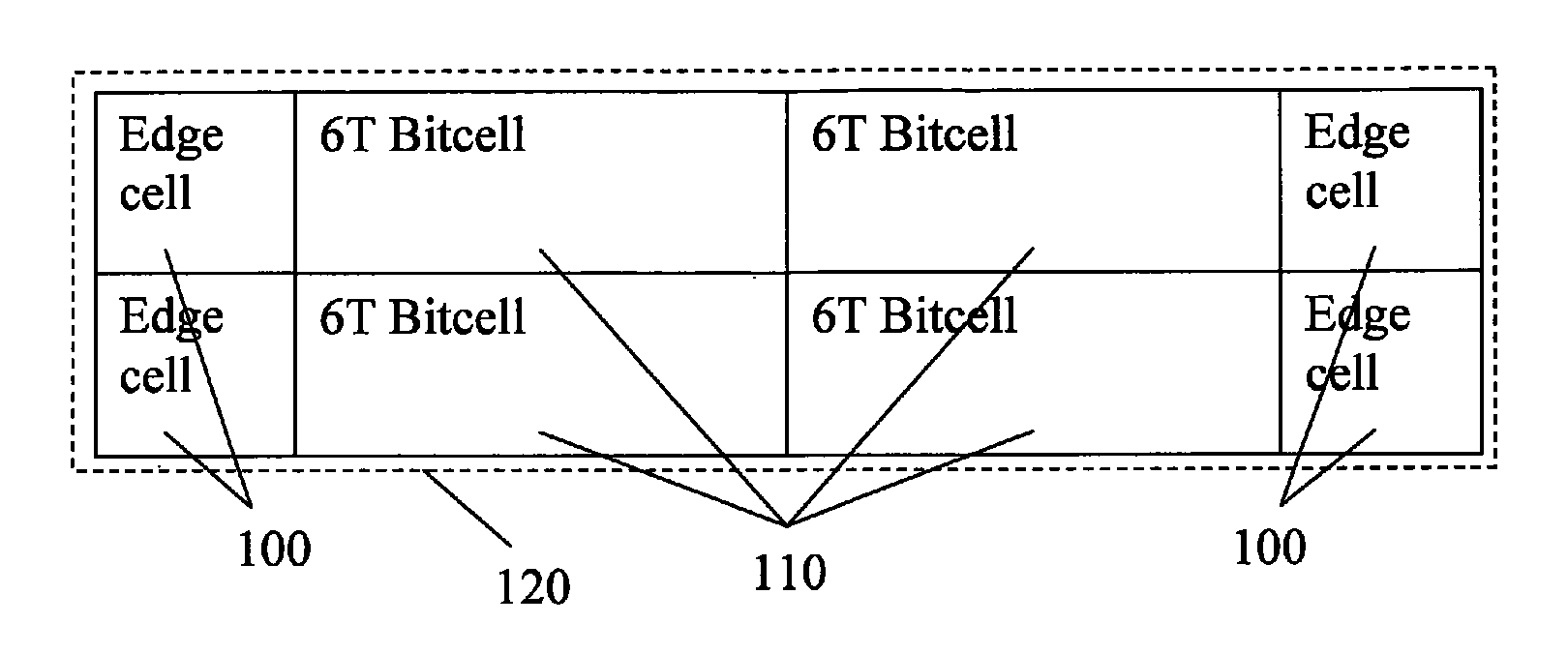
[0020]An example of the base layout layers of a preferred embodiment of the pushed rule bit cell with new functionality of the present invention is illustrated in FIG. 6. Active layer geometries are denoted by a dotted pattern 440FIG. 6. Polysilicon geometries are denoted by a crosshatch pattern 430FIG. 6. In the preferred embodiment the bit cell has the functionality of a TCAM bit cell 50 illustrated in FIG. 2. The TCAM bit cell 460FIG. 6 is constructed from a 6T SRAM bit-cell layout 450FIG. 6, a mirrored 6T SRAM bit-cell layout 400FIG. 6, a half compare cell layout 420FIG. 6, and a mirrored half compare cell layout 410FIG. 6.

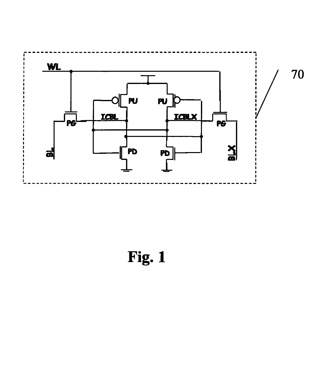
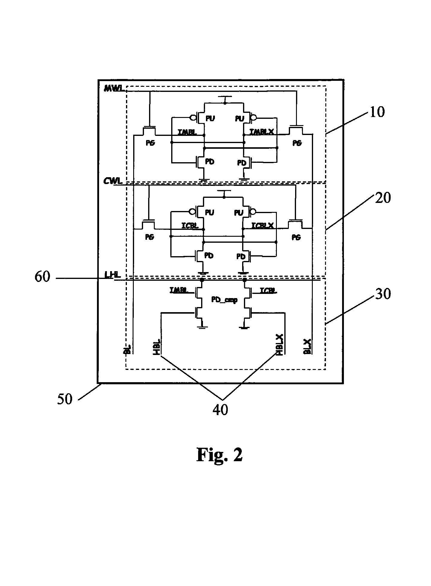
[0021]A 6T bit-cell schematic 70 is illustrated in FIG. 1. The TCAM bit-cell schematic 50 in FIG. 2 is composed of three parts: two 6T bit cells 10 and 20, and one compare circuit 30. FIG. 4 illustrates a TCAM bit-cell floor plan showing the TCAM bit cell 220 to be composed of two 6T SRAM bit cells 200 arrayed wit...


PUM


Abstract

A memory bit cell suitable for use in semiconductor integrated circuits that utilizes pushed design rules and layout geometries optimized by a semiconductor foundry for standard memory bit cells and edge-cell structures that provides a different functionality from that provided by the foundry standard bit cell. This different functionality is achieved by interconnecting the elements of one or a plurality of standard foundry bit cells and edge cells to implement a different circuit with different operation from the original bit cells and edge cells. The positioning and interconnection of the standard bit cells and edge cells are implemented in a manner so as to maintain the same periodic geometric proximity effects to the maximum degree possible. A preferred embodiment of this invention is to interconnect two standard foundry six-transistor SRAM bit cells and two edge cells to create a Ternary Content Addressable Memory bit cell with mask and compare functionality in addition to bit storage functionality.

Description

CROSS-REFERENCE TO RELATED APPLICATIONS[0001]This application claims the benefit of provisional patent application entitled Provisional Patent Application for Pushed-rule Bit Cells with New Functionality filed 2008 Nov. 24, Application No. 61 / 200,146 by the present inventor.FEDERALLY SPONSORED RESEARCH[0002]Not ApplicableSEQUENCE LISTING OF PROGRAM[0003]Not ApplicableBACKGROUND OF THE INVENTION[0004]1. Field of Invention[0005]This invention relates to the design and layout of semiconductor memory bit cells using design rules that are smaller than the standard logic design rules for a given process technology node in order to reduce area per bit and improve performance.[0006]2. Prior Art[0007]Prior art for many types of memory bit cells such as Content Addressable Memories (CAMs) and Register File Memories use bit cells laid out using the standard logic design rules for a given process technology node such as 28-nanometer. This has the advantage that the design rules are proven to pr...

Claims


Application Information

Patent Timeline
Patent Type & Authority Patents(United States)
IPC IPC(8): G11C15/00
CPCG11C15/04
Inventor ZAMPAGLIONE, MICHAEL ANTHONY
Owner SYNOPSYS INC
Why Eureka
Try Eureka