Structure and method for power field effect transistor

a technology of power field effect transistor and structure, which is applied in the direction of semiconductor devices, solid-state devices, basic electric elements, etc., can solve the problems of consuming too much space of pre-formed cans, unable to reach ever lower values of parasitic electrical parameters, and inflexible use of specific chip sizes for allowing the assembly and packaging of inverted mosfet chips or of stacked chips, etc., to achieve the effect of saving pcb area, thin contours,

Active Publication Date: 2013-01-22
TEXAS INSTR INC
View PDF2 Cites 10 Cited by
  • Summary
  • Abstract
  • Description
  • Claims
  • Application Information

AI Technical Summary

Benefits of technology

[0005]Applicant recognized that the market trends in electronic devices, which incorporate power switches, demand thin, light weight and low cost products, amenable to integration with stacked chips of field effect transistors (MOSFETs) and parts such as capacitors and inductors. As a consequence, the structure of the packages for the power switches has to be compatible with mounting the FETs by single terminal, by two terminals, and as stacked chips. The packages further have to be flexible with regard to footprint and layout on printed circuit boards (PCBs); in addition, the fabrication needs to be simple, very low cost, and amenable for attaching heat sinks.
[0010]It is a technical advantage that a power switch with stacked FETs not only saves PCB area, but can also be produced with thin contours so that parasitic electrical parameters are minimized and electrical characteristics such as device speed can be maximized.
[0011]It is another technical advantage that the stacked configuration of the FETs can be produced as a power switch wherein the common terminal features an independent connection to the PCB. This connection can be utilized to attach an external part such as an energy storing inductor in an integrated manner, producing the type of compact power switch device, which the market requires.
[0012]As yet another technical advantage, an FET assembly with the gate on top, and a stacked FET assembly, allow an easy visual inspection of the PCB assembly, providing a welcome improvement for process control.
[0013]It is a further technical advantage that the size of the insulated mesas of the FET plate can be extended by selective partial etching from both sides of the plate. Extended mesas not only can provide better quality control at surface mount to the PCB, but also reduce the stress in the joints of the board-assembled FET, thus enhancing the reliability of the power FET.
[0014]It is another technical advantage that the FET chips can be produced as hermetic units, rendering the power switch device moisture insensitive.

Problems solved by technology

Applicant found that the use of metal cans formed for specific chip sizes is too inflexible for permitting the assembly and packaging of inverted MOSFET chips or of stacked chips.
Furthermore, the footprint of pre-formed cans consumes too much area of the ever more crammed and valuable PCBs.
The metal thickness required for the cans makes it difficult for the packages to reach ever lower values of parasitic electrical parameters such as inductance.

Method used


Image

  • Structure and method for power field effect transistor
  • Structure and method for power field effect transistor
  • Structure and method for power field effect transistor

Examples


Embodiment Construction

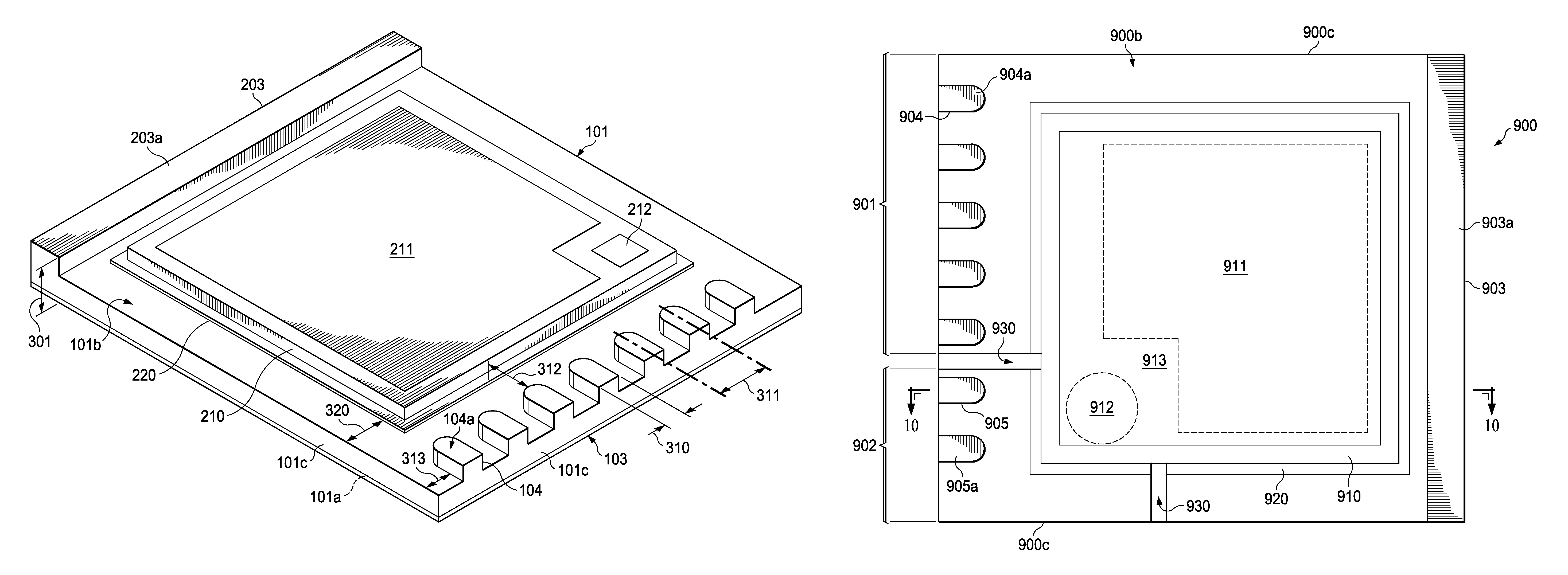
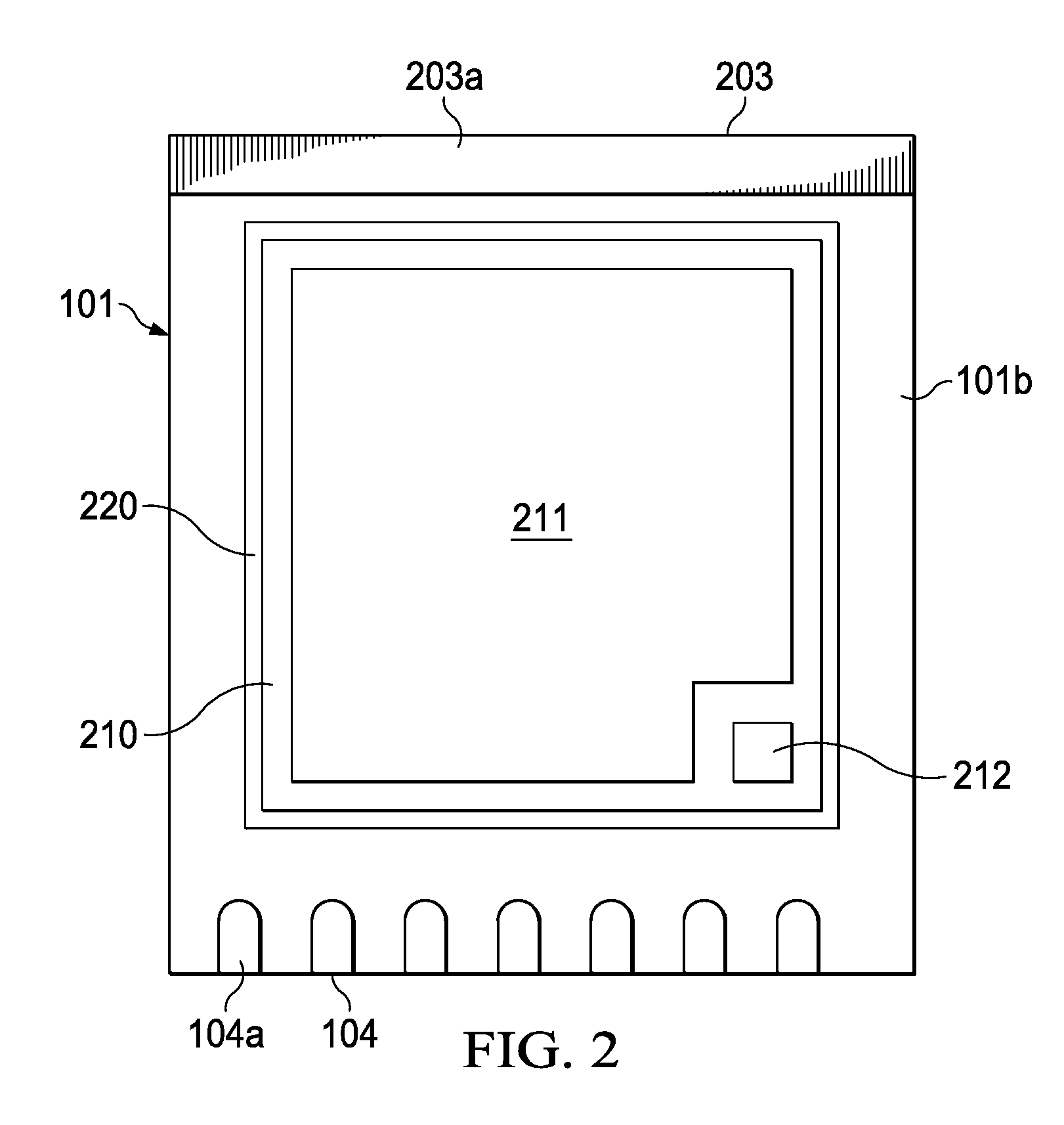
[0029]FIG. 1 depicts an exemplary packaged power field effect transistor (FET), generally designated 100, as an embodiment of the invention. The package includes a metal plate 101 with sawed sides 101c. The preferred metal is copper or a copper alloy; alternatively, aluminum or other metals or compounds with good electrical and thermal conductivities may be used. In the example of FIG. 1, the sides 101c form a square; in other examples, plate 101 may have a rectangular perimeter or any other geometrical outline, which can be sawed from the starting metal strip. The perspective view of FIG. 1 shows the first surface 101a of the plate, indicating that surface 101a is flat to the side corners. In the example of FIG. 1, surface 101a is actually covered by a layer 103 made of a material suitable for device symbolization; exemplary materials include black-colored polymeric compounds based on an epoxy or polyimide formulation.

[0030]FIG. 1 further indicates at least one metal mesa 104 protr...


PUM

PropertyMeasurementUnit
thicknessaaaaaaaaaa
thicknessaaaaaaaaaa
thicknessesaaaaaaaaaa

Abstract

A packaged semiconductor device has a metal plate (1200) with sawed sides (1200c), a flat first surface (1200a) and a parallel second surface (1200b); the plate is separated into a first section (1201) and a second section (1202) spaced apart by a gap (1230). The plate has on the second surface (1200b) at least one insular mesa (1205) of the same metal in each section, the mesas raised from the second plate surface. The device further has an insulating member (1231), which adheres to the first plate surface, bridges the gap, and thus couples the first and second sections together. The device further has a vertical stack (1270) of two power FET chips (1210) and (1220), each having a pair of terminals on the first chip surface (1211 and 1212; 1221 and 1222 respectively) and a single terminal on the second chip surface. The single terminals of chip (1210) and chip (1220) are attached to each other to form the common terminal (1240). The terminal pair (1221) and (1222) is conductively attached to plate (1200) so that terminal (1221) contacts the first plate section (1201) and terminal (1222) contacts the second plate section (1202). The terminal pair (1211) and (1212) is available for attachment to a substrate.

Description

FIELD OF THE INVENTION[0001]The present invention is related in general to the field of semiconductor devices and processes, and more specifically to the structure and fabrication method of power transistors with a terminal formed as packaging plate.DESCRIPTION OF RELATED ART[0002]An essential component of a large number of electronic apparatus is a power switch. To operate properly, a power switch not only needs to have high efficiency, but should preferably have small dimensions and very low cost. A popular power switch involves MOS Field Effect Transistors (FETs), which provide low resistance and can carry large amounts of current; they stay cool by dissipating heat effectively and thus can switch fast (fast transient response). As additional features, the market favors very thin and low cost FETs.[0003]A typical power MOS FET has three terminals: The current flows between the Source and the Drain terminals, and the Gate terminal turns this flow on or off. It is common to produce...

Claims


Application Information

Patent Timeline
Patent Type & Authority Patents(United States)
IPC IPC(8): H01L23/538H01L23/52H01L21/60B44C1/22
CPCH01L23/492H01L23/645H01L24/33H01L24/73H01L25/074H01L25/16Y10T29/49117H01L23/49568H01L23/60H01L24/29H01L2224/16H01L2224/73153H01L2224/73203H01L2224/73253H01L2924/01013H01L2924/01027H01L2924/01029H01L2924/01046H01L2924/01047H01L2924/0105H01L2924/01078H01L2924/01079H01L2924/01082H01L2924/01322H01L2924/014H01L2924/078H01L2924/13091H01L2924/14H01L2924/19041H01L2924/19042H01L2924/19043H01L2924/19107H01L2924/30107H01L2924/01006H01L2924/01033H01L2224/32245H01L23/49562Y10T29/49204Y10T29/49121H01L2924/1305H01L2924/1306H01L2924/3512H01L2924/00H01L2924/12042H01L24/40H01L2224/0558H01L2224/05573H01L2224/05568H01L2224/05124H01L2224/05147H01L2224/05155H01L2224/05644H01L2224/05664H01L24/41H01L2224/37147H01L24/37Y10T83/0443H01L2224/0603H01L2224/04026H01L2224/06181H01L2224/33181H01L2224/04034H01L24/06H01L2224/0401H01L24/05H01L24/84H01L2224/84801H01L2224/83801H01L24/83H01L2924/00014
Inventor KODURI, SREENIVASAN K
Owner TEXAS INSTR INC
Why Eureka
Try Eureka