Floating gate inverter type memory cell and array

a floating gate inverter and memory cell technology, applied in semiconductor devices, solid-state devices, instruments, etc., can solve the problems of not being able to operate ultra-low power and imposing limitations, and achieve the effect of improving the layout of non-volatile memory cells and small layout area

Active Publication Date: 2013-02-19
TOWER SEMICONDUCTOR
View PDF15 Cites 153 Cited by
  • Summary
  • Abstract
  • Description
  • Claims
  • Application Information

AI Technical Summary

Benefits of technology

[0010]Accordingly, the present invention provides a non-volatile memory cell that is fabricated in accordance with a single-poly CMOS logic process. In accordance with a first embodiment, a non-volatile memory cell of the present invention includes a floating gate, which supports a control capacitor, a tunnel capacitor and a floating gate (FG) CMOS inverter structure for implementing read operations. The floating gate CMOS inverter structure includes a pull-up transistor having a source coupled to a pull-up voltage supply, and a pull-down transistor having a source coupled to a pull-down voltage supply. The floating gate forms the gate electrodes of the pull-up and pull-down transistors. The drain of the pull-up transistor is connected directly to a first select transistor, and the drain of the pull-down transistor is connected directly to a second select transistor, such that the drains of the pull-up and pull-down transistors are not directly connected to one another. By eliminating the common connection between the drains of the pull-up and pull-down transistors, the resulting non-volatile memory cell advantageously eliminates a pair of contacts that are required in conventional non-volatile memory cells that use the CMOS inverter principle for readout. The elimination of these contacts allows for an improved layout of the non-volatile memory cells in an array, such that the array exhibits a relatively small layout area.
[0011]In one variation, the memory cell is fabricated in a semiconductor substrate having a first conductivity type. The control capacitor and the tunnel capacitor of the memory cells are fabricated in isolated well regions of the first conductivity type, which in turn, are fabricated in deep well regions of a second conductivity type. In another variation, the control capacitor and the tunnel capacitor are fabricated in well regions of the second conductivity type, without requiring deep well structures.
[0012]In accordance with a second embodiment, a non-volatile memory cell of the present invention includes a floating gate, which supports a control capacitor and a floating gate (FG) CMOS inverter structure for implementing program, erase and read operations. The floating gate CMOS inverter structure includes a PMOS pull-up transistor and an NMOS pull-down transistor. The PMOS pull-up transistor is fabricated in an n-well region, which in turn, is fabricated in a first deep n-well region. The NMOS pull-down transistor is fabricated in a first isolated p-well region, which is fabricated in the first deep n-well region. The control capacitor includes a counter-electrode implemented by a second isolated p-well region, which is fabricated in a second deep n-well region. Program and erase operations are performed by F-N tunneling, by applying program and erase voltages to the first and second isolated p-well regions. Advantageously, a dedicated tunnel capacitor is not required by the second embodiment, thereby minimizing the required memory cell layout area.

Problems solved by technology

Despite the mentioned advantages, Roizin et al. and Sarig undesirably require a relatively large layout area per cell, while Turner et al. does not allow for ultra-low power operation and requires special circuitry to transfer high voltages for programming.
These limitations become pronounced when high volumes of logic memory cells are requested.

Method used


Image

  • Floating gate inverter type memory cell and array
  • Floating gate inverter type memory cell and array
  • Floating gate inverter type memory cell and array

Examples


first embodiment

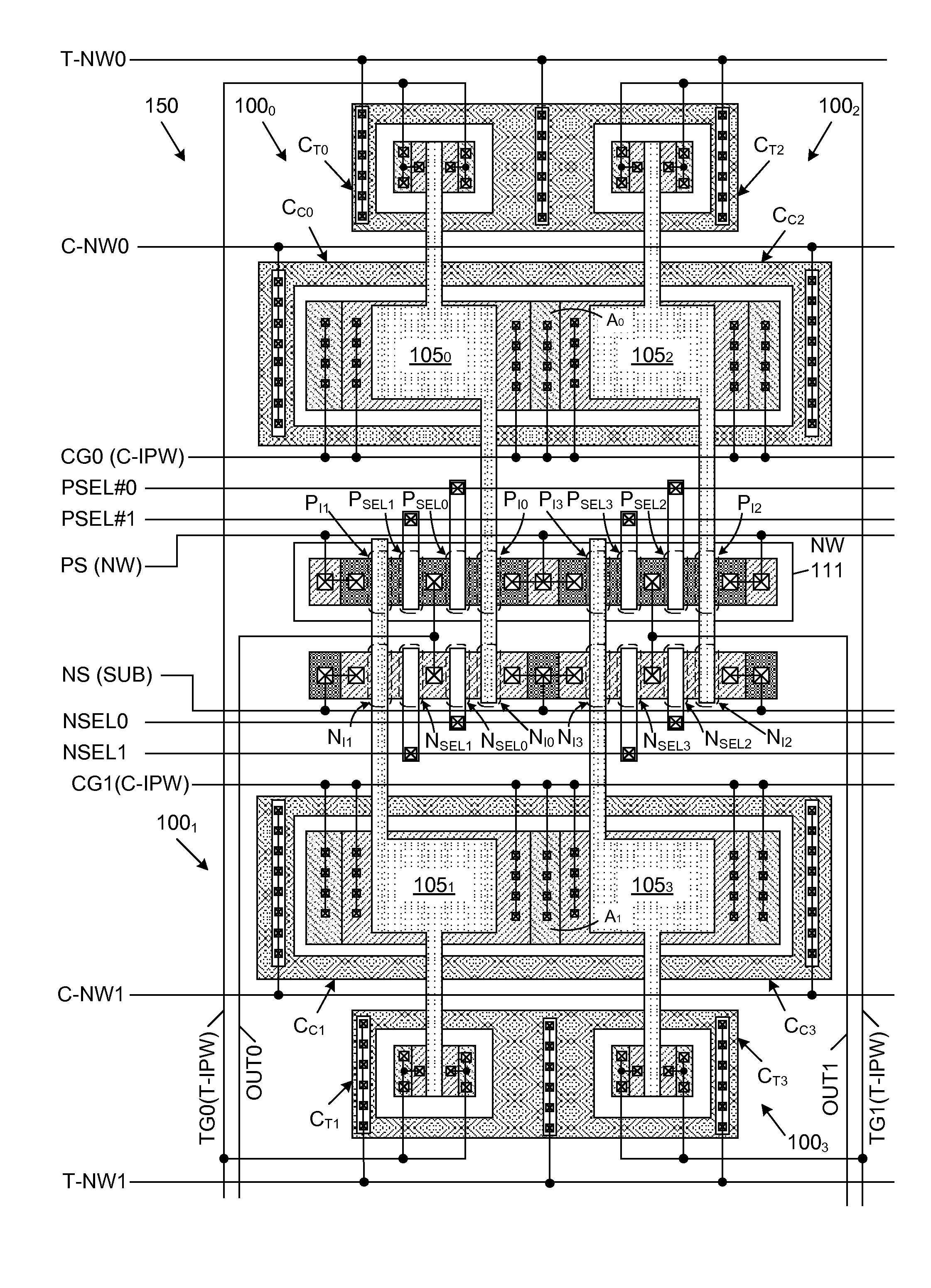
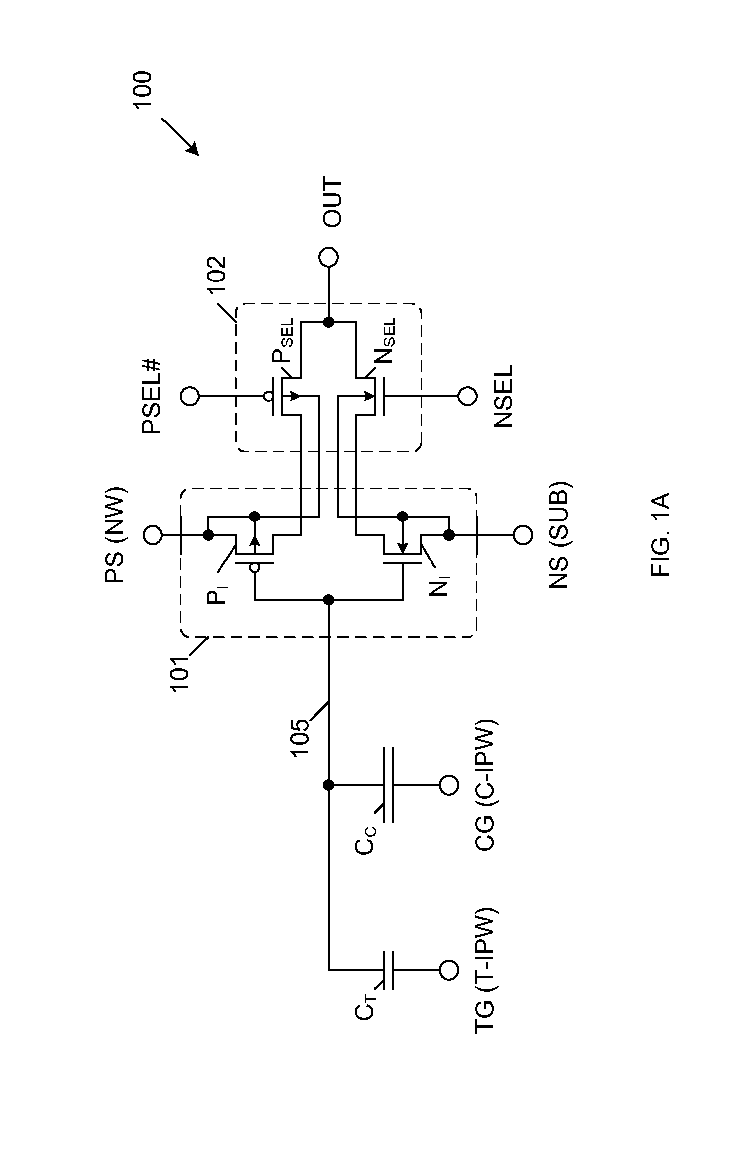
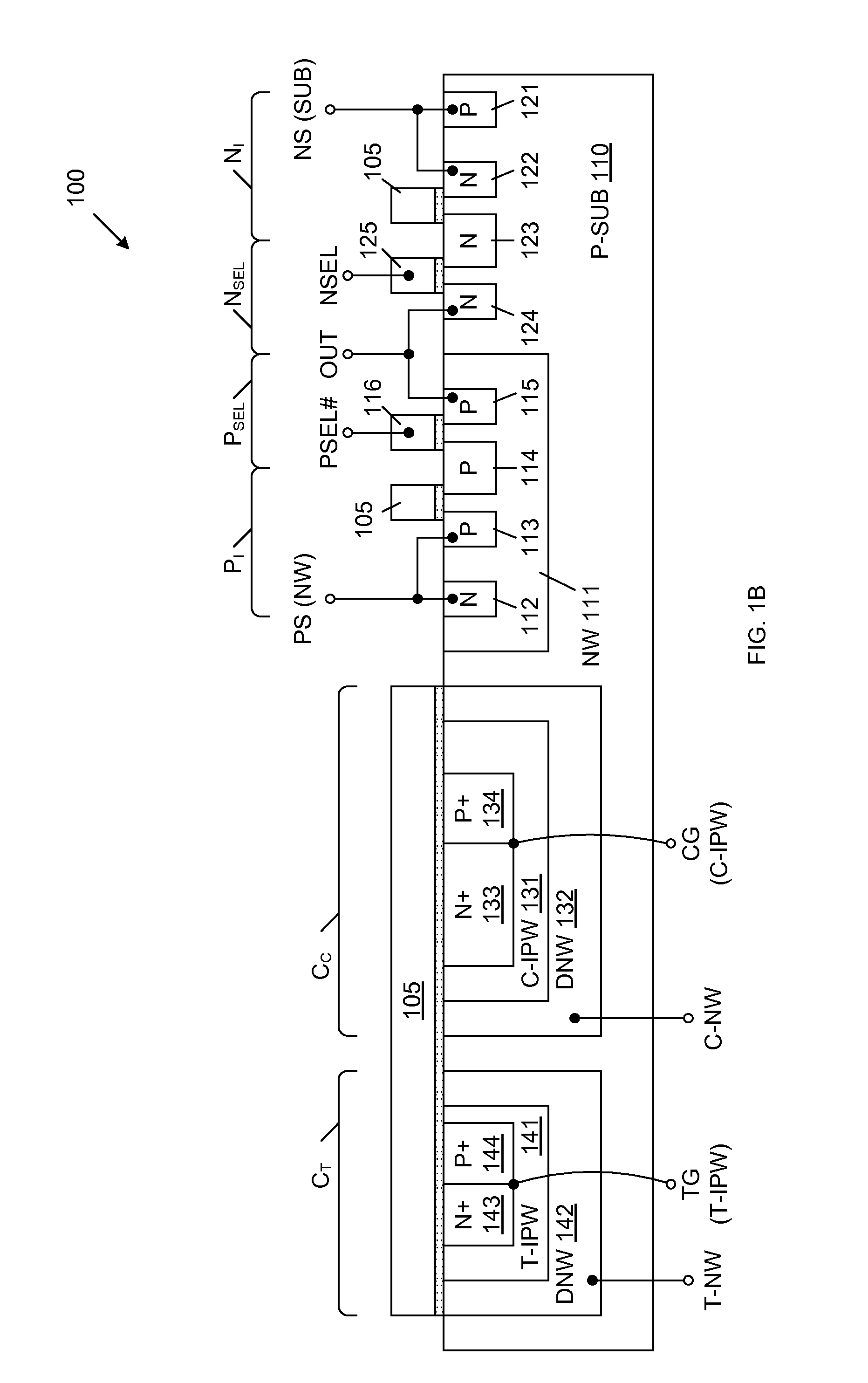
[0031]FIG. 1A is a circuit diagram of a single-poly non-volatile memory cell 100 in accordance with a first embodiment of the present invention. Memory cell 100 includes tunnel capacitor CT, control capacitor CC, CMOS inverter circuit 101, and read output circuit 102. CMOS inverter circuit 101 includes PMOS pull-up transistor PI and NMOS pull-down transistor NI. Read output circuit 102 includes PMOS select transistor PSEL and NMOS select transistor NSEL. Tunnel capacitor CT, control capacitor CC, PMOS pull-up transistor PI and NMOS pull-down transistor NI share a common floating gate electrode 105. That is, floating gate electrode 105 forms the gates of PMOS pull-up transistor PI and NMOS pull-down transistor NI, and also forms the electrodes of tunnel capacitor CT and control capacitor CC. In the described embodiments, floating gate electrode 105 is conductively doped polysilicon, which is fabricated in accordance with a conventional single-poly CMOS logic process. The counter-elec...

second embodiment

[0077]In accordance with an alternate embodiment of the present invention, the tunnel capacitor CT is eliminated from memory cell 100, and the NMOS transistors NI and NSET are located in an isolated p-well region (IPW). Also in this embodiment, the NMOS pull-down transistor NI of the CMOS inverter 101 (i.e., the NMOS pull-down transistor NII of the CMOS inverter circuit 201, below) serves as an injection capacitor in the program and erase modes. Also in this embodiment, the PMOS pull-up transistor PI of the CMOS inverter 101 (i.e., the PMOS pull-up transistor PII of the CMOS inverter circuit 201, below) serves as an injection capacitor in the erase mode. A significant reduction in the required memory cell layout area is achieved due to the elimination of the tunnel capacitor CT. In a particular embodiment, the required layout area of the memory cell can be reduced from about 55 um2 to about 33 um2. This alternate embodiment is described in more detail below in connection with FIGS. ...


PUM


Abstract

A non-volatile memory (NVM) cell and array includes a control capacitor, tunneling capacitor, CMOS inverter and output circuit. The CMOS inverter includes PMOS and NMOS inverter transistors. The control capacitor, tunneling capacitor and PMOS and NMOS inverter transistors share a common floating gate, which is programmed / erased by Fowler-Nordheim tunneling. The output circuit includes PMOS and NMOS select transistors. The PMOS inverter and select transistors share a common source / drain region. Similarly, the NMOS inverter and select transistors share a common source / drain region. This configuration minimizes the required layout area of the non-volatile memory cell and allows design of arrays with smaller footprints. Alternately, the tunneling capacitor may be excluded, further reducing the required layout area of the NVM cell. In this case, the NMOS inverter transistor functions as a tunneling capacitor for programming and erasing the cell, and the PMOS inverter transistor functions as a tunneling capacitor for erasing the cell.

Description

RELATED APPLICATIONS[0001]This application is a continuation in part of U.S. patent application for “Single Poly CMOS Logic Memory Cell For RFID Application And Its Programming And Erasing Method”, U.S. application Ser. No. 11 / 936,718, filed Nov. 7, 2007, which claims priority of U.S. Provisional patent application for “Single Poly CMOS Logic Memory Cell For RFID Application And Its Programming And Erasing Method”, U.S. App. Ser. No. 60 / 869,081, filed Dec. 7, 2006.FIELD OF THE INVENTION[0002]This invention relates to complimentary metal-oxide-silicon (CMOS) integrated circuit (IC) devices, and more particularly to memories for passive radio frequency identification (RFID) CMOS IC devices and other mobile applications.RELATED ART[0003]It is desirable for embedded non-volatile memory devices to exhibit low power consumption in all operational states: programming, erasing, and readout. In particular applications (e.g., RFID), the currents utilized to facilitate the operational states o...

Claims


Application Information

Patent Timeline
Patent Type & Authority Patents(United States)
IPC IPC(8): H01L29/788
CPCG11C16/0441H01L27/115H01L27/11519H01L27/11521H01L27/11558G11C2216/10H10B69/00H10B41/10H10B41/30H10B41/60
Inventor AUDZEYEU, MIKALAIMAKAREVICH, YURIYSHVEDAU, SIARHEIBELOUS, ANATOLYPIKHAY, EVGENYDAYAN, VLADISLAVROIZIN, YAKOV
Owner TOWER SEMICONDUCTOR
Why Eureka
Try Eureka