Borderless contact for ultra-thin body devices

a contact structure and ultra-thin body technology, applied in the field of semiconductoroninsulator (etsoi) devices with borderless contact, can solve the problems of inability to meet the requirements of high-speed communication, and the leakage current is unacceptabl

Active Publication Date: 2013-02-26
GLOBALFOUNDRIES U S INC
View PDF13 Cites 14 Cited by
  • Summary
  • Abstract
  • Description
  • Claims
  • Application Information

AI Technical Summary

Problems solved by technology

While ETSOI devices, and especially ETSOI field effect transistors (FETs), are promising candidates for advanced high performance devices, several manufacturing issues need to be resolved before ETSOI devices can be manufactured with high yield.
One such issue is formation of divots around and / or over shallow trench isolation structures that are employed to provide lateral electrical isolation between adjacent devices.
For example, silicon oxide-based shallow trench isolation structures are susceptible to HF-based etches that can be employed to preclean semiconductor surfaces before epitaxy or formation of a gate dielectric.
Even if a direct electrical short is avoided, a conductive material deposited in divots can lead to an unacceptable level of leakage current between a portion of the bottom semiconductor layer and an electrical node that should be electrically isolated from the bottom semiconductor layer.

Method used


Image

  • Borderless contact for ultra-thin body devices
  • Borderless contact for ultra-thin body devices
  • Borderless contact for ultra-thin body devices

Examples


first embodiment

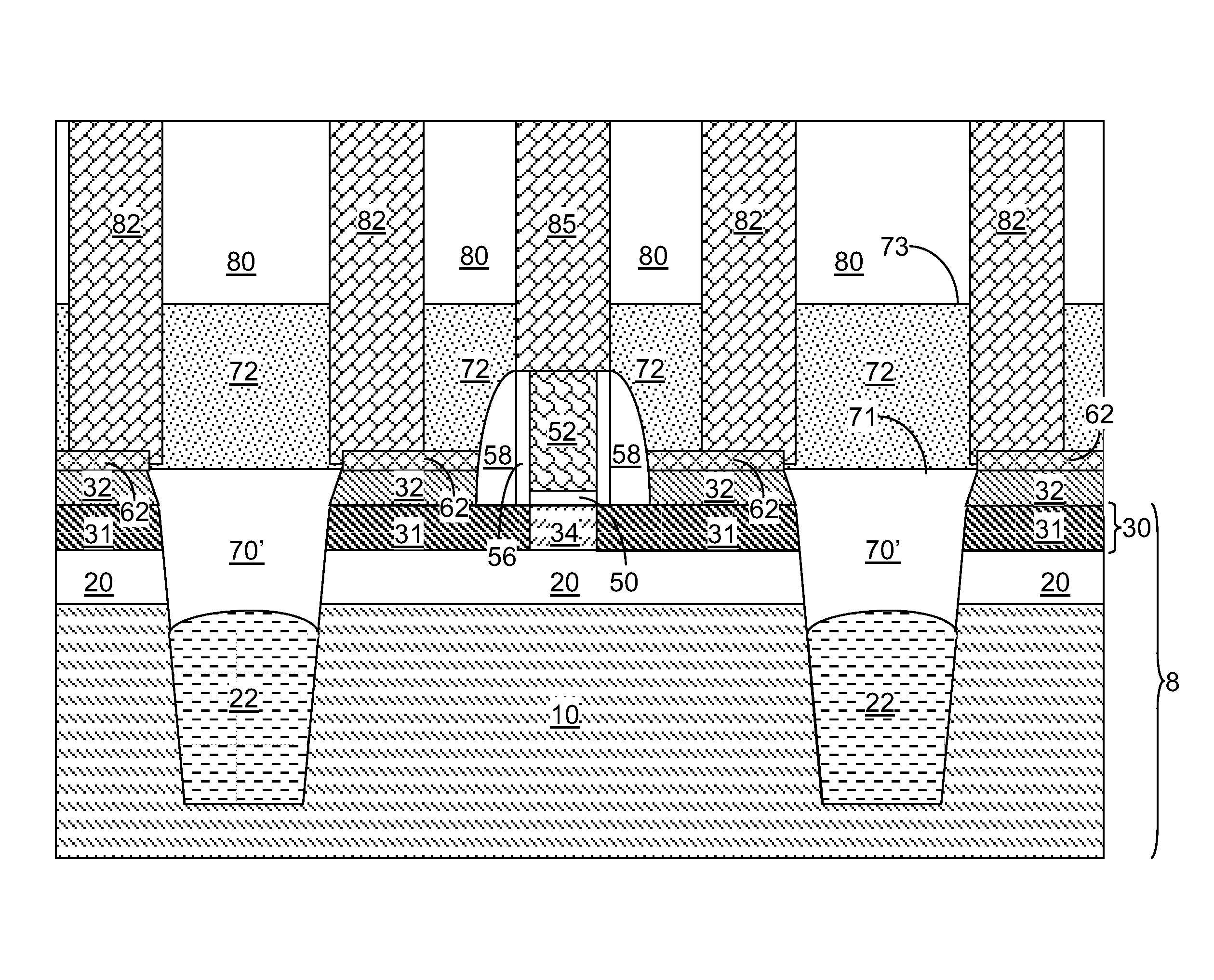
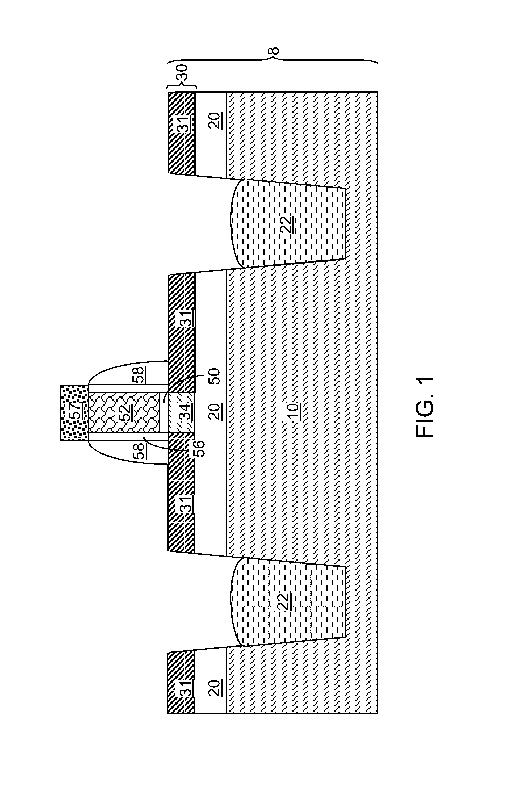
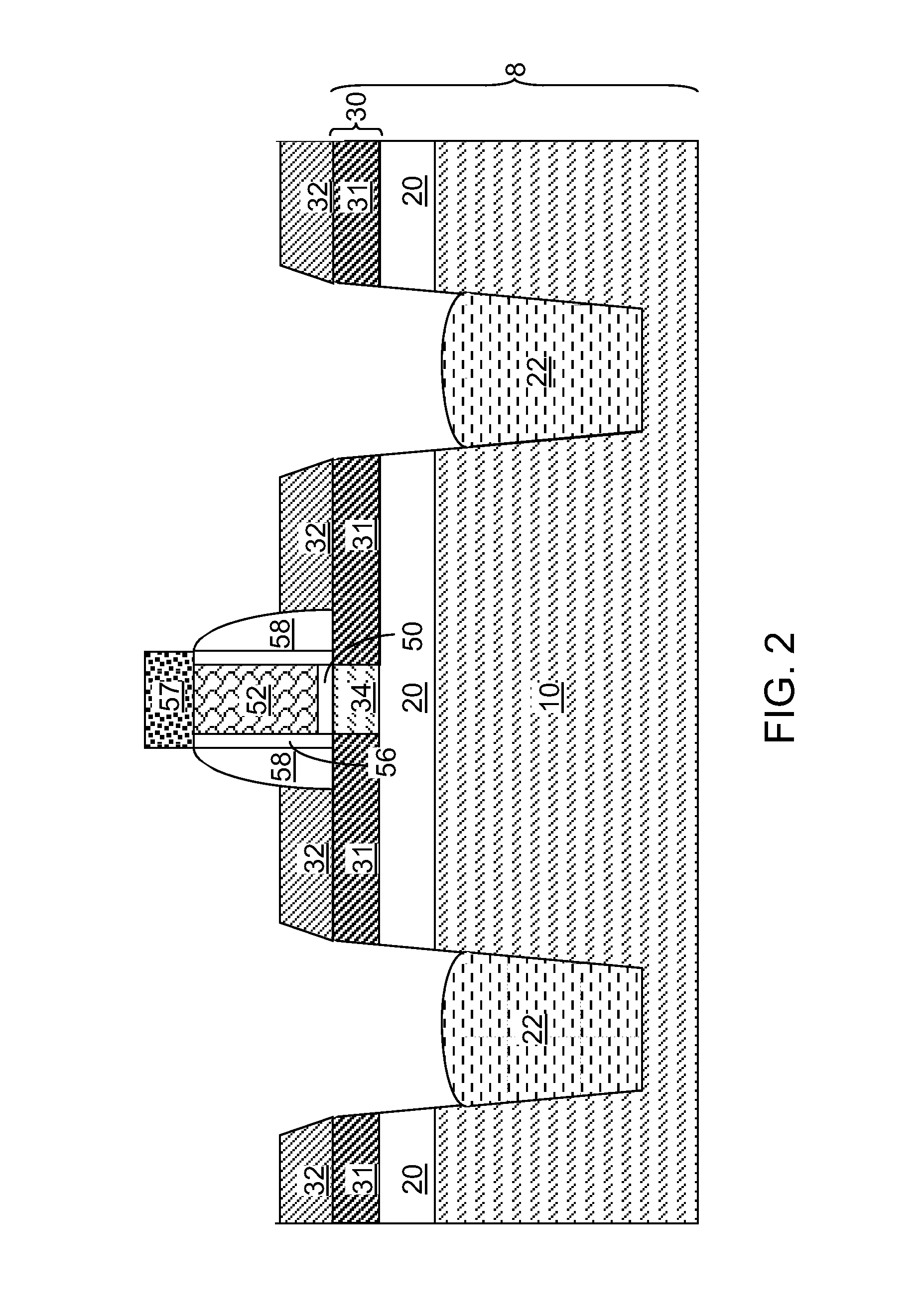
[0026]Referring to FIG. 1, a first exemplary semiconductor structure according to the present disclosure includes gate-level layers formed on a semiconductor substrate 8. The substrate 8 can be a semiconductor-on-insulator (SOI) substrate including a vertical stack of a handle substrate 10, a buried insulator layer 20, and a top semiconductor layer 30. The handle substrate 10 can include a semiconductor material, a dielectric material, a conductive material, or a combination thereof. For example, the handle substrate 10 can be a single crystalline silicon substrate. The buried insulator layer 20 includes a dielectric material such as silicon oxide, silicon nitride, silicon oxynitride, or a combination thereof. The top semiconductor layer 30 includes a semiconductor material such as silicon, germanium, a silicon-germanium alloy, a III-V compound semiconductor, a II-VI compound semiconductor, any other semiconductor material known in the art, or combinations thereof. The semiconductor...

second embodiment

[0058]Referring to FIG. 9, a second exemplary semiconductor structure according to the present disclosure can be derived from the first exemplary semiconductor structure of FIG. 3 by depositing a first dielectric layer 170. The first dielectric layer 170 is a dielectric material layer including a first dielectric material. The first dielectric layer 170 can be a conformal dielectric layer that can be deposited, for example, by chemical vapor deposition (CVD).

[0059]The first dielectric layer 170 is deposited directly on the top surface of the shallow trench isolation structures 22 and various top surfaces of components of the semiconductor device. For example, the first dielectric layer 170 can be deposited directly on source / drain metal semiconductor alloy regions 62, the gate spacers 58, and the gate cap dielectric 57 of a field effect transistor. In one embodiment, if the top surface of the shallow trench isolation structures 22 are recessed below the top surface of the handle sub...


PUM


Abstract

After formation of a semiconductor device on a semiconductor-on-insulator (SOI) layer, a first dielectric layer is formed over a recessed top surface of a shallow trench isolation structure. A second dielectric layer that can be etched selective to the first dielectric layer is deposited over the first dielectric layer. A contact via hole for a device component located in or on a top semiconductor layer is formed by an etch. During the etch, the second dielectric layer is removed selective to the first dielectric layer, thereby limiting overetch into the first dielectric layer. Due to the etch selectivity, a sufficient amount of the first dielectric layer is present between the bottom of the contact via hole and a bottom semiconductor layer, thus providing electrical isolation for the ETSOI device from the bottom semiconductor layer.

Description

BACKGROUND[0001]The present disclosure relates to semiconductor structures, and particularly to a borderless contact structure for extremely thin semiconductor-on-insulator (ETSOI) devices and methods of manufacturing the same.[0002]Extremely thin semiconductor-on-insulator (ETSOI) devices refer to semiconductor devices formed on an extremely thin semiconductor-on-insulator (ETSOI) substrate. A typical ETSOI substrate has a top semiconductor layer, which is also referred to as an extremely thin semiconductor-on-insulator (ETSOI) layer, having a thickness from 5 nm to 50 nm. A buried insulator layer provided underneath the top semiconductor layer has a thickness from 10 nm to 100 nm. An ETSOI substrate can be employed to form various semiconductor devices that derive performance advantage through the reduced thickness of the top semiconductor layer and / or the reduced thickness of the buried insulator layer compared with normal semiconductor-on-insulator (SOI) substrate.[0003]For exam...

Claims


Application Information

Patent Timeline
Patent Type & Authority Patents(United States)
IPC IPC(8): H01L21/76
CPCH01L21/84H01L27/1203H01L29/41783H01L29/66628H01L21/76283H01L29/78609H01L21/76897H01L21/76832H01L21/76834H01L29/665H01L29/7843H01L29/0653H01L29/7841
Inventor FAN, SU CHENHARAN, BALASUBRAMANIAN S.HORAK, DAVID V.
Owner GLOBALFOUNDRIES U S INC
Why Eureka
Try Eureka