Method for manufacturing positive electrode and power storage device
a technology of positive electrodes and power storage devices, which is applied in the manufacture of final products, sustainable manufacturing/processing, cell components, etc., can solve the problems of changing the crystal structure crystal defect etc., to suppress the formation of decomposition products, suppress the reaction between oxygen and the decomposition product, and suppress the decomposition of lithium cobalt oxide
- Summary
- Abstract
- Description
- Claims
- Application Information
AI Technical Summary
Benefits of technology
Problems solved by technology
Method used
Image
Examples
embodiment 1
[Embodiment 1]
[0038]In this embodiment, a power storage device according to one embodiment of the present invention and a manufacturing method thereof will be described.
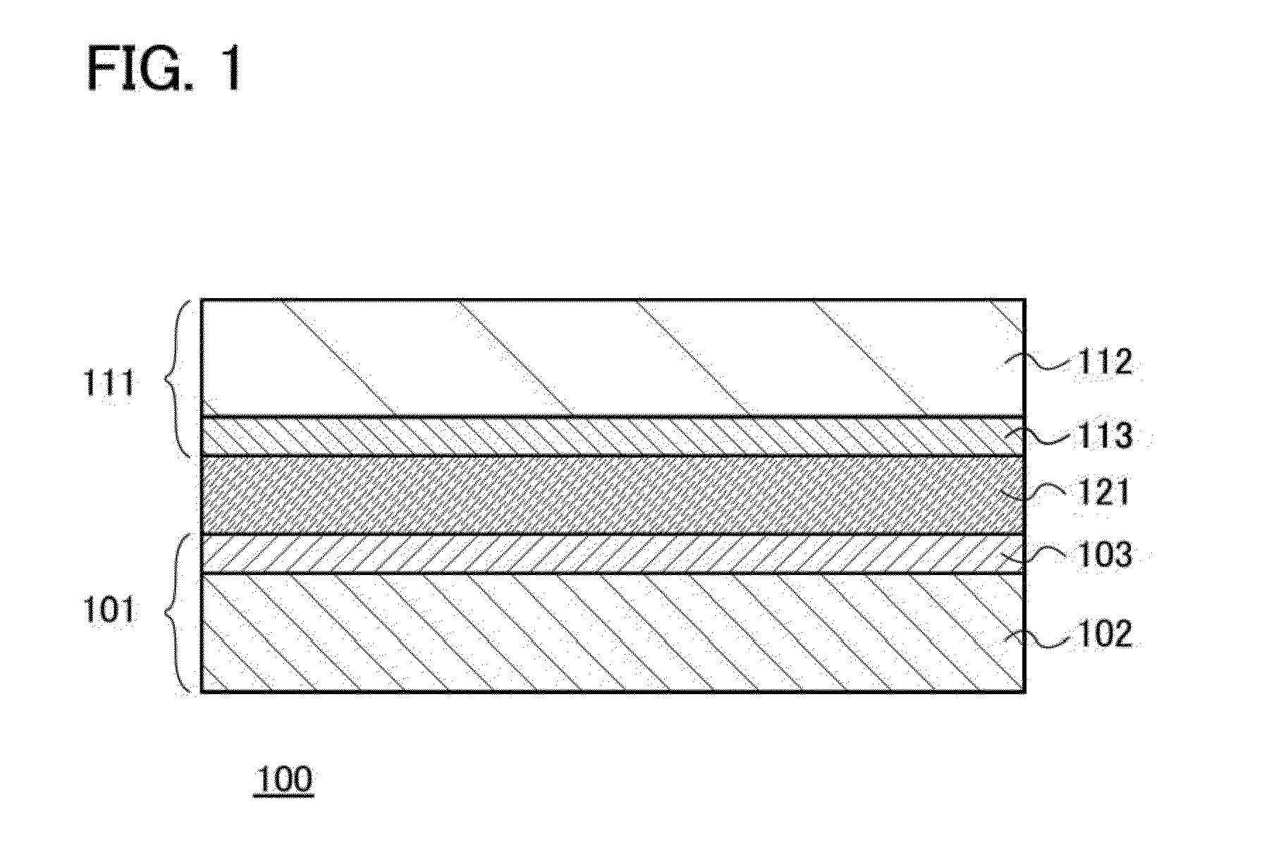
[0039]A power storage device according to this embodiment will be described with reference to FIG. 1. Here, a cross-sectional structure of a secondary battery as a power storage device will be described below.
[0040]Among secondary batteries, a lithium-ion battery formed using a lithium-containing metal oxide has high capacity and a high level of safety. Here, the structure of a lithium-ion battery, which is a typical example of secondary batteries, will be described.
[0041]FIG. 1 is a cross-sectional view of a power storage device 100.
[0042]The power storage device 100 includes a negative electrode 101, a positive electrode 111, and an electrolyte 121 sandwiched between the negative electrode 101 and the positive electrode 111. In addition, the negative electrode 101 may include a negative electrode current collector ...
embodiment 2
[Embodiment 2]
[0108]In this embodiment, a power storage device having a structure different from that in Embodiment 1 will be described.
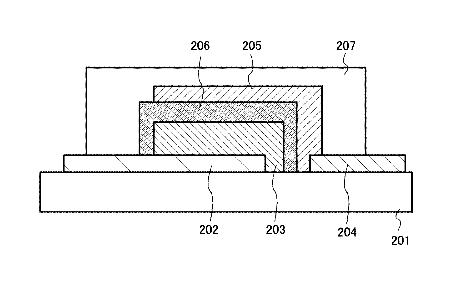
[0109]A power storage device in FIG. 9A includes a substrate 201, and a positive electrode current collector 202 and a negative electrode current collector 204 which are over the substrate 201. A positive electrode active material layer 203 is formed over the substrate 201 and the positive electrode current collector 202. A solid electrolyte layer 206 is formed in contact with the positive electrode current collector 202 so as to cover the positive electrode active material layer 203. A negative electrode active material layer 205 is formed in contact with the solid electrolyte layer 206 and the negative electrode current collector 204. A protective film 207 is formed in contact with the positive electrode current collector 202 and the negative electrode current collector 204 so as to cover the solid electrolyte layer 206 and the negative electrode ...
PUM
| Property | Measurement | Unit |
|---|---|---|
| temperature | aaaaa | aaaaa |
| temperature | aaaaa | aaaaa |
| thickness | aaaaa | aaaaa |
Abstract
Description
Claims
Application Information


