Crystallization methods for preparing group IBIIIAVIA thin film solar absorbers

a technology of solar absorber and semiconductor film, which is applied in the direction of basic electric elements, electrical apparatus, semiconductor devices, etc., can solve the problems of insufficient conversion efficiency of solar cells, difficult process of controlling doping cigs with na, and non-uniformity of cigs layers

Inactive Publication Date: 2013-03-26
SOLOPOWER
View PDF4 Cites 15 Cited by
  • Summary
  • Abstract
  • Description
  • Claims
  • Application Information

AI Technical Summary

Problems solved by technology

This is, however, an uncontrolled process and can cause non-uniformities in the CIGS layers depending on how much Na diffuses from the substrate through the Mo-contact layer.
However when such Na-containing layers are used for CIGS doping, both the small amounts used, often not more than 2 atomic percent, and the high diffusivity of Na at CIGS reaction temperatures make controlled doping CIGS with Na a challenging pr

Method used


Image

  • Crystallization methods for preparing group IBIIIAVIA thin film solar absorbers
  • Crystallization methods for preparing group IBIIIAVIA thin film solar absorbers
  • Crystallization methods for preparing group IBIIIAVIA thin film solar absorbers

Examples


Embodiment Construction

[0025]Various embodiments of the present invention provide methods to form doped Group IBIIIAVIA semiconductor films or layers on continuous flexible substrates or bases, which may be used in the formation of solar cells or photovoltaic cells.

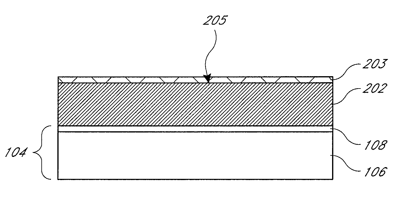
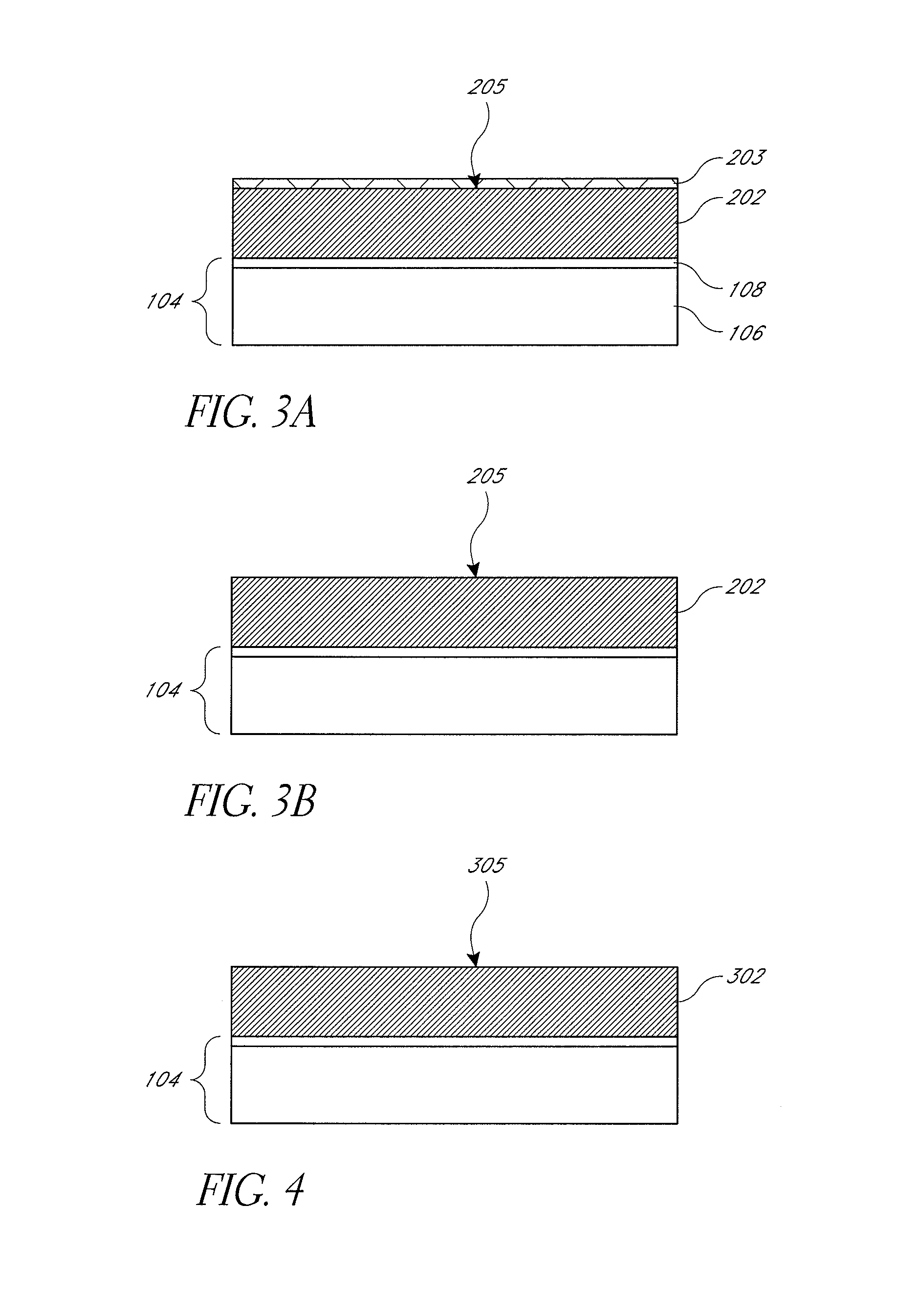
[0026]In one embodiment, the crystallization step or reaction step that forms a doped CIGS absorber is carried out using thermal annealing techniques at high temperatures. A CIGS precursor including for example Group IA dopant elements is annealed at high temperatures to form the doped CIGS layer. At CIGS absorber reaction temperatures, a portion of the Group IA elements such as Na, K or Li may not be used for doping and may be expelled from the CIGS absorber matrix, resulting in these elements accumulating at the CIGS absorber surface as a dopant rich film at the end of the reaction process.

[0027]This dopant rich film at the absorber surface may deteriorate not only the properties of the absorber layer and its surface but also the properties o...


PUM


Abstract

The present invention provides methods for forming a doped Group IBIIIAVIA absorber layer for a solar cell. The method includes forming precursor layers that include a dopant rich layer and then annealing the precursor layers. The annealing process results in dopants diffusing through the layers to an exterior surface. The annealing process is periodically halted to remove dopants from the exposed surface.

Description

BACKGROUND OF THE INVENTION[0001]1. Field of the Invention[0002]The present invention relates to methods and apparatus for preparing thin films of Group IBIIIAVIA compound semiconductor films, and more specifically to reacting of Group IBIIIAVIA compound semiconductor films to form photovoltaic devices.[0003]2. Description of the Related Art[0004]Solar cells are photovoltaic (PV) devices that convert sunlight directly into electrical energy. Solar cells can be based on crystalline silicon or thin films of various semiconductor materials that are usually deposited on low-cost substrates, such as glass, plastic, or stainless steel.[0005]Thin film based photovoltaic cells, such as amorphous silicon, cadmium telluride, copper indium diselenide or copper indium gallium diselenide based solar cells offer improved cost advantages by employing deposition techniques widely used in the thin film industry. Group IBIIIAVIA compound photovoltaic cells, including copper indium gallium diselenide ...

Claims


Application Information

Patent Timeline
IPC IPC(8): H01L21/00
CPCH01L31/0322H01L31/03928H01L31/0323Y02E10/541
Inventor AKSU, SERDARPINARBASI, MUSTAFA
Owner SOLOPOWER
Why Eureka
Try Eureka