Method of removing back metal from an etched semiconductor scribe street

Active Publication Date: 2013-05-28
SEMICON COMPONENTS IND LLC +1
View PDF40 Cites 21 Cited by
  • Summary
  • Abstract
  • Description
  • Claims
  • Application Information

AI Technical Summary

Benefits of technology

[0005]This invention teaches a method of effectively removing

Problems solved by technology

Both result in a significant loss of material during the cutting process.
In addition, both sawing and laser scribing cause damage along the cut edges of the devices that can result in

Method used


Image

  • Method of removing back metal from an etched semiconductor scribe street
  • Method of removing back metal from an etched semiconductor scribe street
  • Method of removing back metal from an etched semiconductor scribe street

Examples


Example

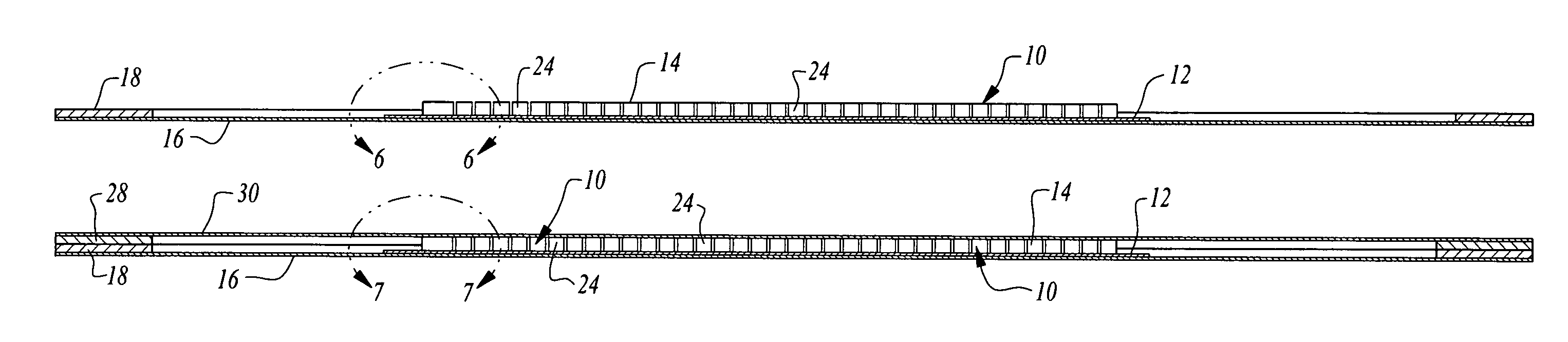
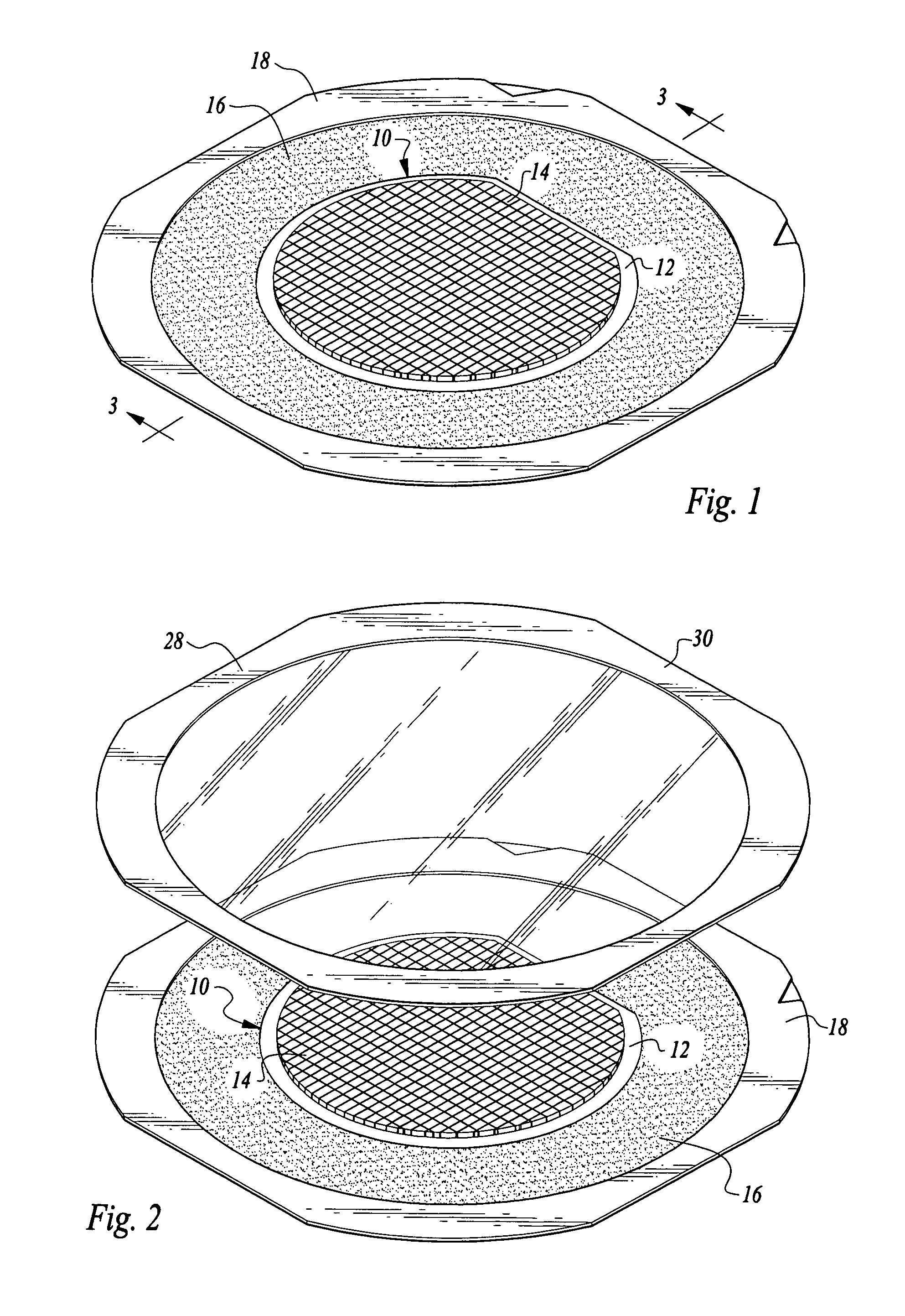
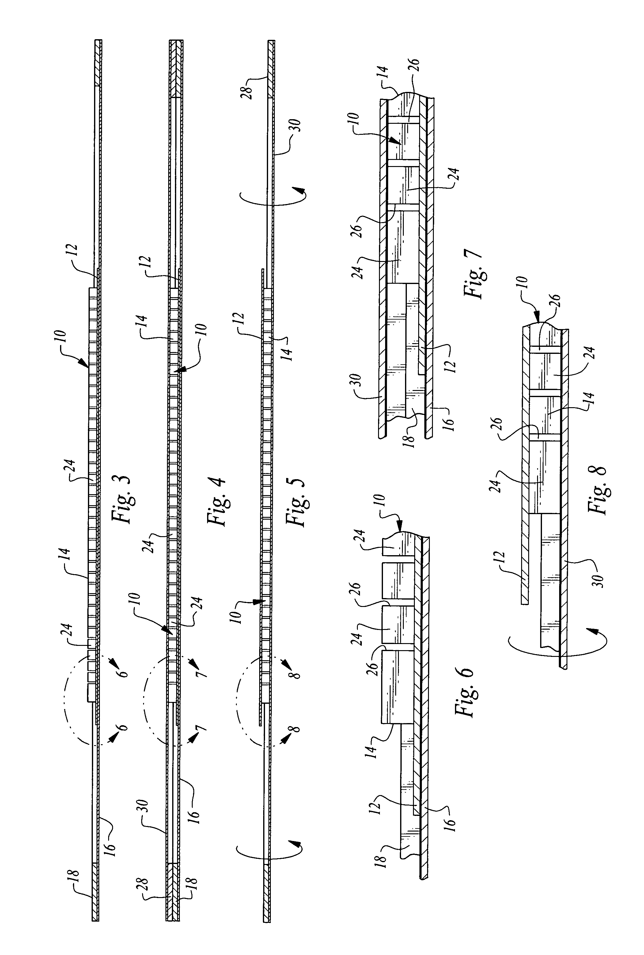
[0027]Referring now to the drawings, a semiconductor wafer 10 is illustrated, the wafer having a metal layer or base 12 and a semiconductor material layer 14. The semiconductor material layer 14 of the wafer shown in FIGS. 1-8 has been etched along scribe streets to form individual semiconductor material dies but leaving the metal layer 12 intact, even in the scribe streets.

[0028]A commercially available etching machine of any suitable type may be employed to etch the semiconductor material to remove semiconductor material in the scribe streets but leaving the metal unetched. That is, the etching process illustrated in FIG. 11 is continued in the normal fashion until the metal layer on the back side of the wafer is reached. U.S. Pat. No. 6,826,840, Lindsey, et al. discloses an apparatus that has the ability to align scribe streets with the direction of travel of a cutting tool, the ability to move a cutting tool rapidly the length of the scribe streets, and the ability to step preci...


PUM


Abstract

A method of dividing a semiconductor wafer having a metal layer and a semiconductor material layer including the step of cutting the semiconductor material layer along scribe streets without cutting the metal layer, turning over the wafer, and cutting the metal layer along the scribe streets.

Description

TECHNICAL FIELD[0001]This invention relates to a method of separating semiconductor devices from a semiconductor wafer.BACKGROUND OF THE INVENTION[0002]In the past, numerous different methods have been used for singulating or dicing a semiconductor wafer, the process of dividing a semiconductor wafer into individual devices. The two most widely used methods at this time are sawing using a diamond saw blade and laser scribing, using a focused laser beam to cut through the wafer. Neither method is ideal. Both result in a significant loss of material during the cutting process. As the size of semiconductor devices get smaller, the width of the line of lost material during the scribing process becomes comparable to the width of the device. If the width of the line of material lost during the scribing process could be made significantly smaller, many more devices could be made on each wafer, resulting in a large savings in the cost of fabricating the devices. In addition, both sawing and...

Claims


Application Information

Patent Timeline
IPC IPC(8): H01L21/00
CPCH01L21/78H01L21/6836H01L2221/68381H01L2221/68327H01L2221/6834H01L2221/68318
Inventor LINDSEY, JR., PAUL C.
Owner SEMICON COMPONENTS IND LLC
Why Eureka
Try Eureka