Clock-data recovery and method for binary signaling using low resolution ADC
a clock-data recovery and binary signal technology, applied in the field of signal detection, can solve the problems of small eye opening and easy error by receivers
- Summary
- Abstract
- Description
- Claims
- Application Information
AI Technical Summary
Benefits of technology
Problems solved by technology
Method used
Image


Examples
embodiment 200
[0026]FIG. 2 depicts a functional block diagram of an embodiment 200 of a clock-data recovery (CDR) circuit in accordance with the present invention. CDR circuit 200 comprises: a variable-gain amplifier (VGA) 210 for amplifying an input signal with a gain factor controlled by a gain setting to generate an amplified signal; a low-resolution ADC (analog-digital converter) 220 for converting the amplified signal into 3-bit data D[2:0] in accordance with a timing provided by a recovered clock; a 4-level slicer 280 for slicing the 3-bit data D[2:0] into a 2-bit slicer output data S[1:0]; a timing detection circuit 240 for processing the 2-bit slicer output data S[1:0] to generate a timing error signal; a filter 260 for filtering the timing error signal to generate a control voltage; a VCO (voltage controlled oscillator) 250 for generating the recovered clock under a control of the control voltage; an AGC (automatic gain control) block 270 for processing the 2-bit slicer output data S[1:0...
embodiment 640
[0060]Now refer to FIG. 6A. For a high frequency application, the unit-delay circuits 610 and 620 need to operate at a high clock frequency. For instance, for a 5 Gigabit-per-second link, the unit-delay circuits 610 and 620 need to operate at 5 GHz. A straight implementation using 5 GHz clock may not be easily practical. In this case, one can use a serial-to-parallel conversion to convert the serial 3-bit data D[2:0] into a block of 3-bit data at a lower frequency and perform block signal processing, as shown in embodiment 640 of FIG. 6B. The high frequency clocked 3-bit converter output data D[2:0] is converted into a block of lower frequency clock data by the S / P block 642 using a lower frequency clock. For instance, the serial 3-bit converter output data D[2:0] at 5 GHz can be converted into a block of twenty parallel 3-bit dada at 250 MHz. The method for performing such a serial-to-parallel conversion (S / P block 642) is well known to those of ordinary skill in the art and thus n...
embodiment 700
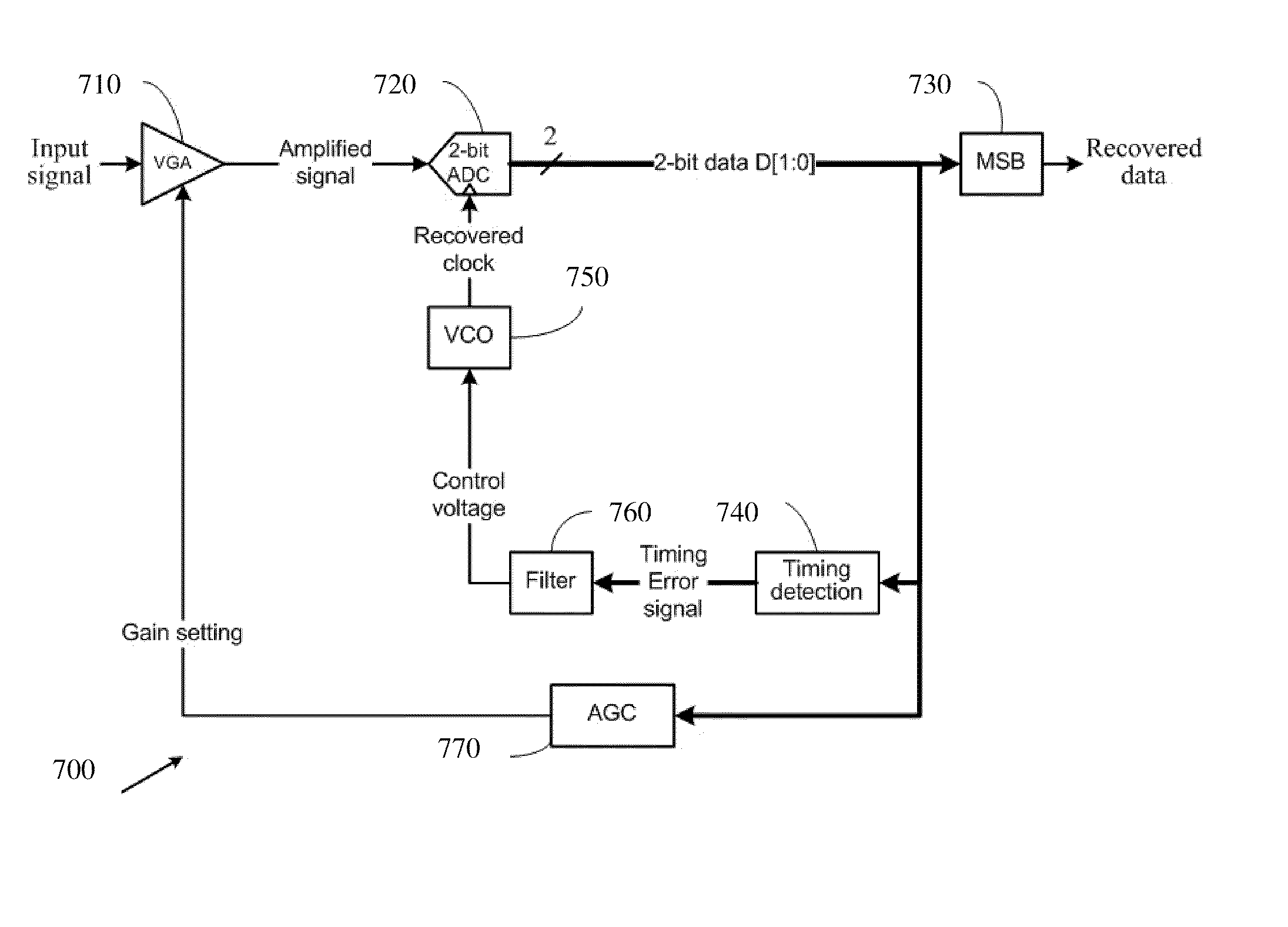
[0062]FIG. 7 depicts a functional block diagram of an embodiment 700 of a clock-data recovery (CDR) circuit in accordance with the present invention. CDR circuit 700 comprises: a variable-gain amplifier (VGA) 710 for amplifying an input signal with a gain factor controlled by a gain setting to generate an amplified signal; a 2-bit ADC (analog-digital converter) 720 for converting the amplified signal into 2-bit data D[1:0] in accordance with a timing provided by a recovered clock; a MSB functional block 730 for extracting the most significant bit of the 2-bit data D[1:0] to form the recovered data; a timing detection circuit 740 for processing the 2-bit data D[1:0] to generate a timing error signal; a filter 760 for filtering the timing error signal to generate a control voltage; a VCO (voltage controlled oscillator) 750 for generating the recovered clock under a control of the control voltage; and an AGC (automatic gain control) block 770 for processing the 2-bit data D[1:0] to gen...
PUM
 Abstract
Description
Claims
Application Information