Semiconductor device
a technology of semiconductors and semiconductors, applied in the direction of digital storage, capacitors, instruments, etc., can solve the problems of long time-consuming data storage, achieve the effect of reducing power consumption, ensuring data integrity, and ensuring data integrity
- Summary
- Abstract
- Description
- Claims
- Application Information
AI Technical Summary
Benefits of technology
Problems solved by technology
Method used
Image
Examples
embodiment 1
[Embodiment 1]
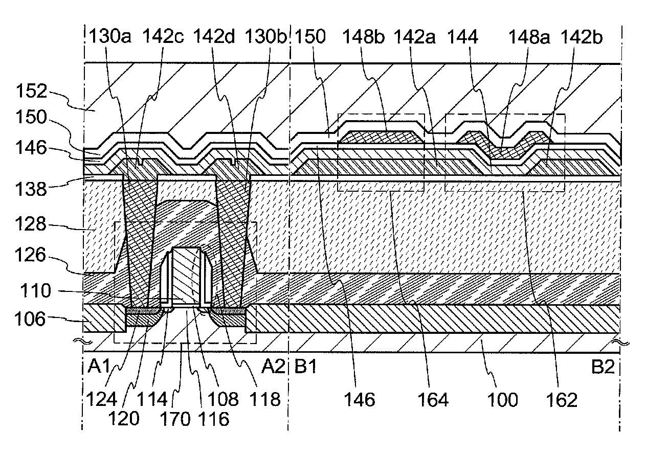
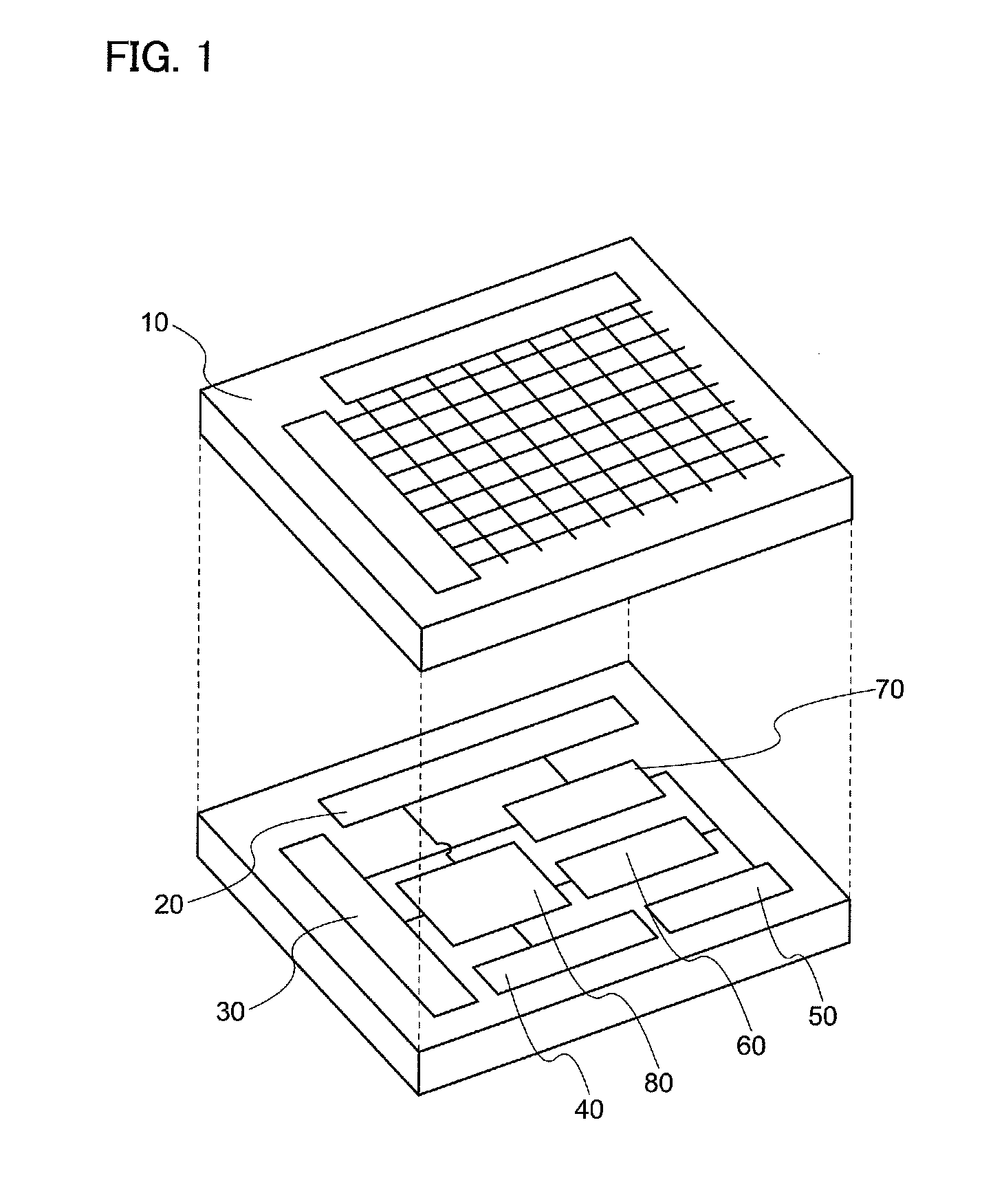
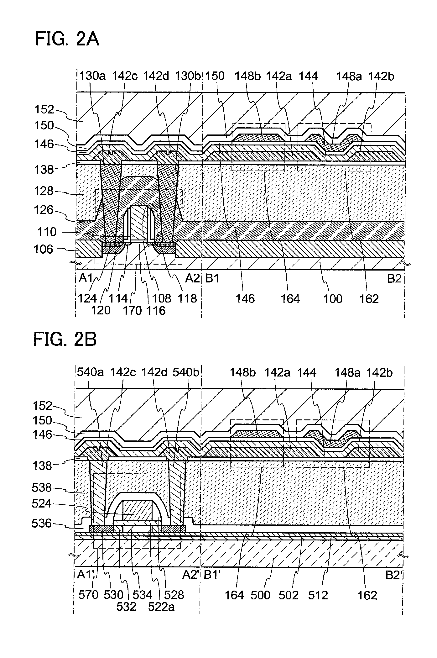
[0047]In this embodiment, structures and a manufacturing method of a semiconductor device according to one embodiment of the disclosed invention will be described with reference to FIG. 1, FIGS. 2A and 2B, FIGS. 3A and 3B, FIGS. 4A to 4C, and FIGS. 5A1, 5A2, and 5B. Note that in some of the circuit diagrams, “OS” is written beside a transistor in order to indicate that the transistor uses an oxide semiconductor.
[0048]FIG. 1 is a schematic view illustrating an example of a structure of a semiconductor device. A semiconductor device according to one embodiment of the disclosed invention is, typically, a semiconductor device with a layered structure which includes a memory circuit in an upper portion and a logic circuit (also referred to as an arithmetic circuit) and a driver circuit which need high speed operation in a lower portion.
[0049]A semiconductor device illustrated in FIG. 1 is a semiconductor device (a memory device) including a memory cell array 10 in an upper ...
embodiment 2
[Embodiment 2]
[0105]In this embodiment, a manufacturing method of a semiconductor device using an oxide semiconductor, specifically, a manufacturing method of the transistor 162 in an upper portion in FIGS. 2A and 2B is described with reference to FIGS. 6A to 6E. Note that since FIGS. 6A to 6E are cross-sectional views mainly illustrating the manufacturing steps and the like of the transistor 162, detailed description of the transistor 170 and the like below the transistor 162 is omitted.
[0106]First, the insulating layer 138 is formed over the interlayer insulating layer 128. After that, a conductive layer is formed over the insulating layer 138 and is selectively etched, so that the source or drain electrode 142a and the source or drain electrode 142b are formed (see FIG. 6A).
[0107]The insulating layer 138 functions as a base and can be formed by a PVD method, a CVD method, or the like. The insulating layer 138 can be formed using a material containing an inorganic insulating mater...
embodiment 3
[Embodiment 3]
[0144]In this embodiment, a manufacturing method of a transistor using an oxide semiconductor (especially, an oxide semiconductor having an amorphous structure) will be described with reference to FIGS. 7A to 7E. The transistor can be used instead of the transistor 162 or the like in any of the above embodiments. A structure of the transistor according to this embodiment and the structure of the transistor according to any of the above embodiments are partly common to each other. Therefore, a difference is mainly described below. A top-gate transistor is described below as an example; however, a structure of the transistor is not limited to a top-gate structure.
[0145]First, an insulating layer 202 is formed over an object 200. After that, an oxide semiconductor layer 206 is formed over the insulating layer 202 (see FIG. 7A).
[0146]The object 200 is, for example, the interlayer insulating layer 128 in any of the above embodiments. Arithmetic mean deviation (Ra) of a surf...
PUM
 Abstract
Description
Claims
Application Information


