
Voltage sensitive resistor (VSR) read only memory

a voltage sensitive resistor and read only technology, applied in the direction of bulk negative resistance effect devices, thin film varistors, instruments, etc., can solve the problems of inability to store the most data in the smallest area, limited real estate on a semiconductor device,

Inactive Publication Date: 2013-06-18
IBM CORP
View PDF13 Cites 1 Cited by
  • Summary
  • Abstract
  • Description
  • Claims
  • Application Information

AI Technical Summary

Benefits of technology

The present invention provides a voltage sensitive resistor (VSR) read only memory (ROM) device that includes a semiconductor device and a VSR. The VSR is made of a CVD titanium nitride layer with residual titanium-carbon bonding that can become less resistive when a predetermined voltage and current are applied. The VSR ROM device is a write once read only memory (WO ROM) device. The invention also provides a method for forming the VSR ROM device on a semiconductor substrate with a semiconductor device. The technical effects of the invention include providing a reliable and efficient memory device for semiconductor devices and improving the programming precision of programmable logic circuits.

Problems solved by technology

Since real estate on a semiconductor device is limited, memory and storage designs that store the most data in the smallest areas are in demand.

Method used


Image

  • Voltage sensitive resistor (VSR) read only memory
  • Voltage sensitive resistor (VSR) read only memory
  • Voltage sensitive resistor (VSR) read only memory

Examples


first embodiment

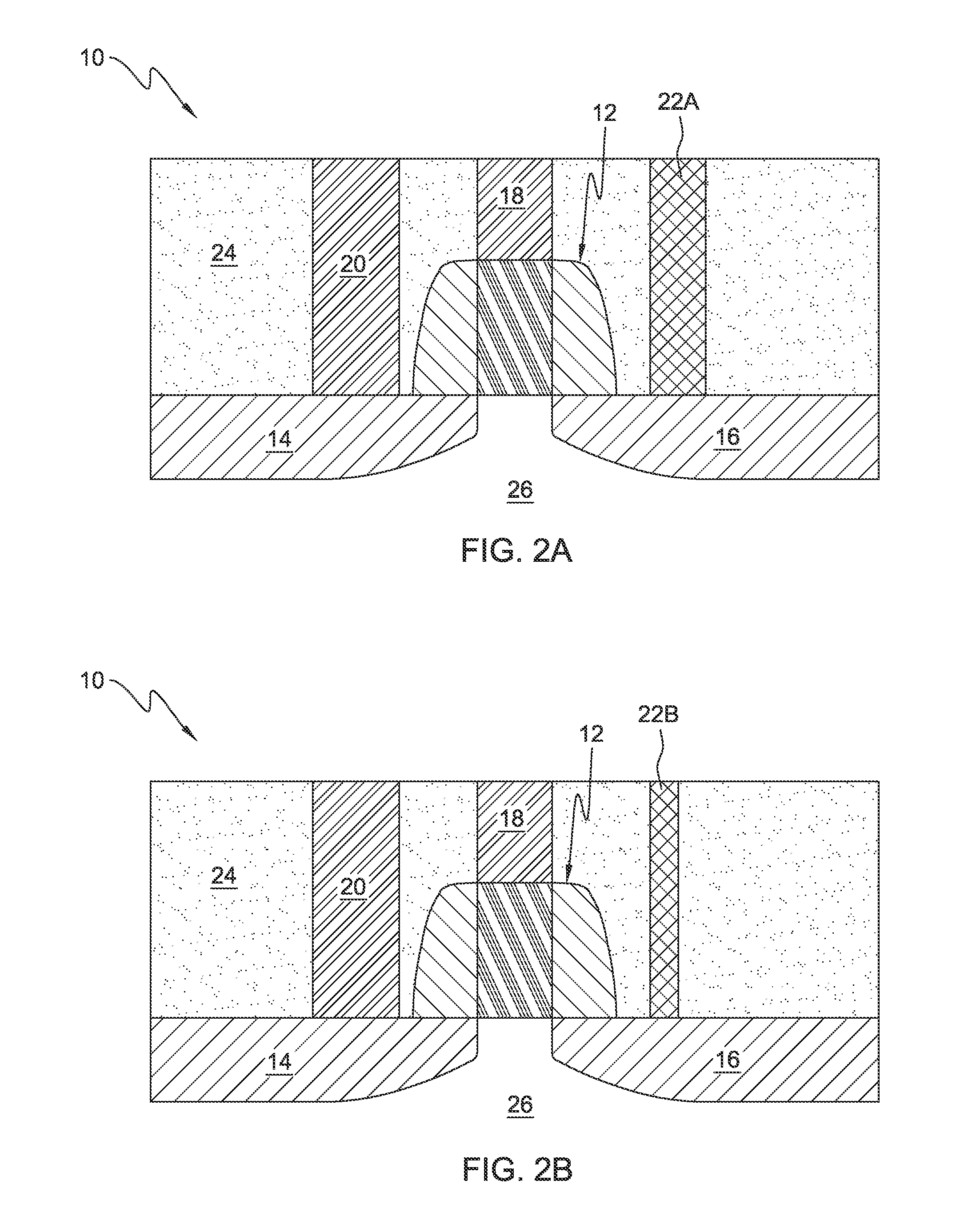
[0025]Referring now to FIG. 2A, there is shown the present invention. Shown in FIG. 2A is a semiconductor 10 which includes the usual gate structure 12, semiconductor material 26, source 14 and drain 16. In contact with the gate structure 12 is a first CA contact 18 and in contact with source 14 is a second CA contact 20. First and second CA contacts 18, 20 are conventional. Also shown in FIG. 2A is a VSR 22A in contact with drain 16 of the semiconductor 10. First and second CA contacts 18, 20 and VSR 22 are embedded in a conventional dielectric material 24 as is known in the art.

second embodiment

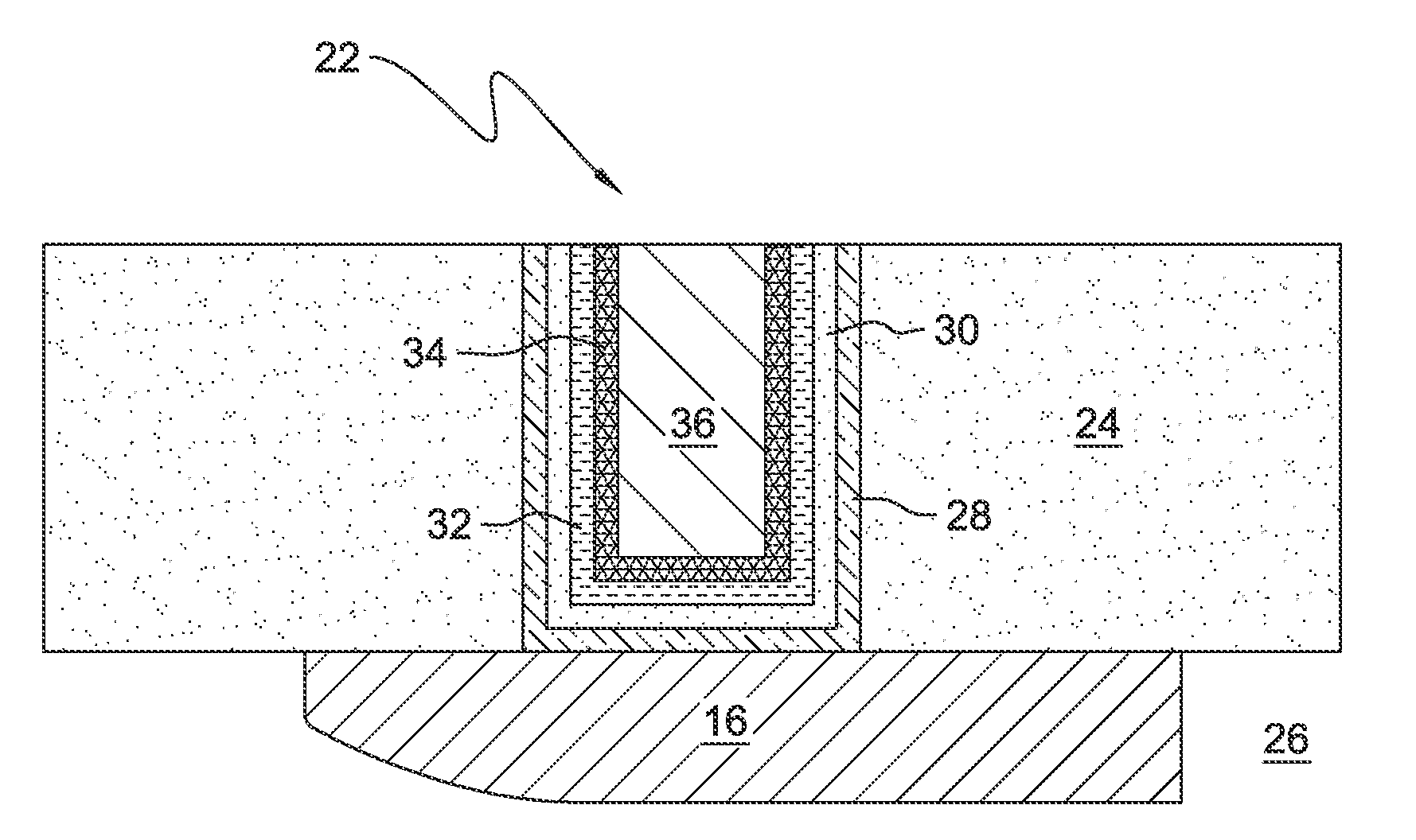
[0026]Referring now to FIG. 2B, there is shown a second embodiment of the present invention. the invention is identical to the first embodiment of the invention except that VSR 22B is smaller. For purposes of illustration and not limitation, VSR 22A may have a via diameter of about 90 nm while VSR 22B may have a via diameter of about 45 nm. The size of the VSR 22A, 22B may affect the processing to form the VSR 22A, 22B as will be explained hereafter. VSR 22A and VSR 22B may collectively hereafter be simply denoted at VSR 22.

[0027]The semiconductor material 26 may be any semiconductor material including but not limited to group IV semiconductors such as silicon, silicon germanium or germanium, a III-V compound semiconductor, or a II-VI compound semiconductor. The semiconductor material may be a bulk semiconductor material or silicon-on-insulator.

[0028]Referring now to FIG. 3, the VSR 22 is shown in a circuit with the semiconductor 10 wherein the VSR 22 is electrically and physically ...


PUM


Abstract

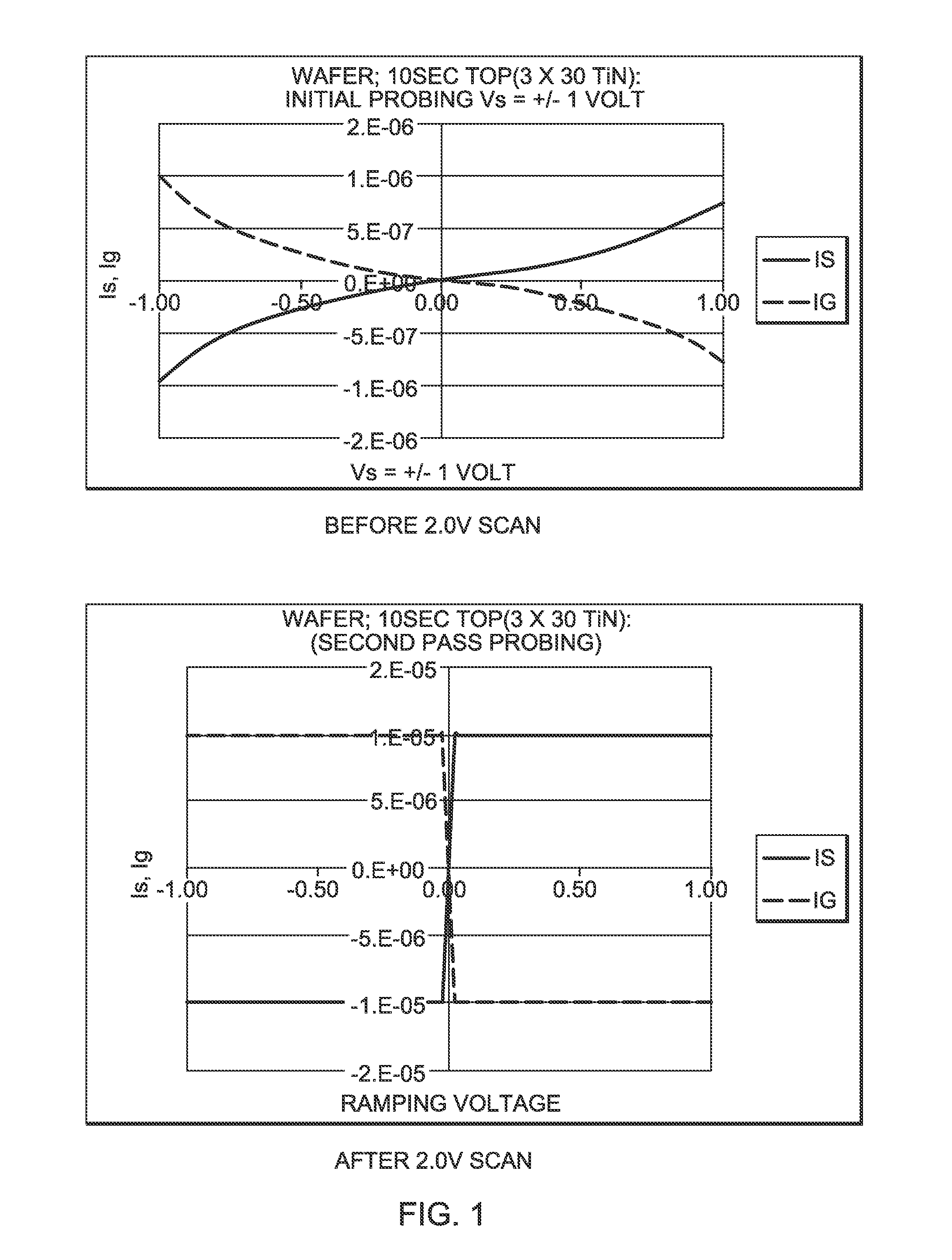
Disclosed is a voltage sensitive resistor (VSR) write once (WO) read only memory (ROM) device which includes a semiconductor device and a VSR connected to the semiconductor device. The VSR WO ROM device is a write once read only device. The VSR includes a CVD titanium nitride layer having residual titanium-carbon bonding such that the VSR is resistive as formed and can become less resistive by an order of 102, more preferably 103 and most preferably 104 when a predetermined voltage and current are applied to the VSR. A plurality of the VSR WO ROM devices may be arranged to form a high density programmable logic circuit in a 3-D stack. Also disclosed are methods to form the VSR WO ROM device.

Description

BACKGROUND OF THE INVENTION[0001]The present invention relates to a nonvolatile semiconductor memory device for nonvolatilely writing data in accordance with the application of a voltage to a voltage sensitive resistor.[0002]Today's computers need to store more data than ever. Consequently, memory and storage devices are very important to the effectiveness of modern computers. Many recent storage devices replace moving parts with solid-state electronics. Since real estate on a semiconductor device is limited, memory and storage designs that store the most data in the smallest areas are in demand. High density memory which stores the most data in the smallest areas is important, and may even be necessary, in many applications.BRIEF SUMMARY OF THE INVENTION[0003]The various advantages and purposes of the present invention as described above and hereafter are achieved by providing, according to a first aspect of the invention, a voltage sensitive resistor (VSR) read only memory (ROM) d...

Claims


Application Information

Patent Timeline
Patent Type & Authority Patents(United States)
IPC IPC(8): H01L29/02
CPCG11C17/14H01C7/1013H01C7/105H01L23/5256H01L45/1616H01L2924/0002H01L2924/00H10N70/023
Inventor KANE, TERENCE L.WANG, YUN-YUWONG, KEITH KWONG HON
Owner IBM CORP
Learn More