Semiconductor device

a technology of semiconductor devices and semiconductors, applied in the field of semiconductor devices, can solve the problems of power consumption, not only operating power consumption, but also standby power consumption, and achieve the effect of reducing the standby power of the semiconductor device and long li

Inactive Publication Date: 2013-06-18
SEMICON ENERGY LAB CO LTD
View PDF147 Cites 26 Cited by
  • Summary
  • Abstract
  • Description
  • Claims
  • Application Information

AI Technical Summary

Benefits of technology

[0008]However, power consumed by a semiconductor device performing intermittent operation means not only operating power consumption but also standby power consumption (also referred to as standby power). Note that here, standby power means power consumption due to a very small amount of current discharged through an element or a circuit which is electrically connected to a battery. In particular, in the semiconductor device capable of controlling intermittent operation, which is disclosed in Patent Document 1, standby power has a high percentage in total power consumption. Therefore, it is important to reduce standby power for reducing power consumption of the semiconductor device.
[0009]Thus, an object of an embodiment of the present invention is to reduce standby power of a semiconductor device.
[0010]Further, an object of an embodiment of the present invention is to achieve a long lifetime of a semiconductor device.
[0013]When a channel formation region of a transistor is formed using the thus highly purified oxide semiconductor, the transistor can operate so that the drain current of the transistor is smaller than or equal to 1×10⁻¹³ [A] in an off state even with a channel width of 10 mm. That is, leakage current can be significantly reduced by application of a highly purified oxide semiconductor to a channel formation region of a transistor.
[0018]A semiconductor device of an embodiment of the present invention includes a functional circuit, a battery, and a transistor controlling electrical connection between the functional circuit and the battery. A channel formation region of the transistor is formed using an oxide semiconductor in which the hydrogen concentration is lowered. Specifically, the hydrogen concentration of the oxide semiconductor is lower than or equal to 5×10¹⁹ (atoms / cm3). Therefore, electric discharge through the transistor can be suppressed by turning off the transistor in a standby state. As a result, standby power of the semiconductor device can be reduced. Further, by suppressing electric discharge of the battery in a standby state, the semiconductor device can have a long lifetime.

Problems solved by technology

However, power consumed by a semiconductor device performing intermittent operation means not only operating power consumption but also standby power consumption (also referred to as standby power).
Note that here, standby power means power consumption due to a very small amount of current discharged through an element or a circuit which is electrically connected to a battery.
In particular, in the semiconductor device capable of controlling intermittent operation, which is disclosed in Patent Document 1, standby power has a high percentage in total power consumption.

Method used


Image

  • Semiconductor device
  • Semiconductor device
  • Semiconductor device

Examples


embodiment 1

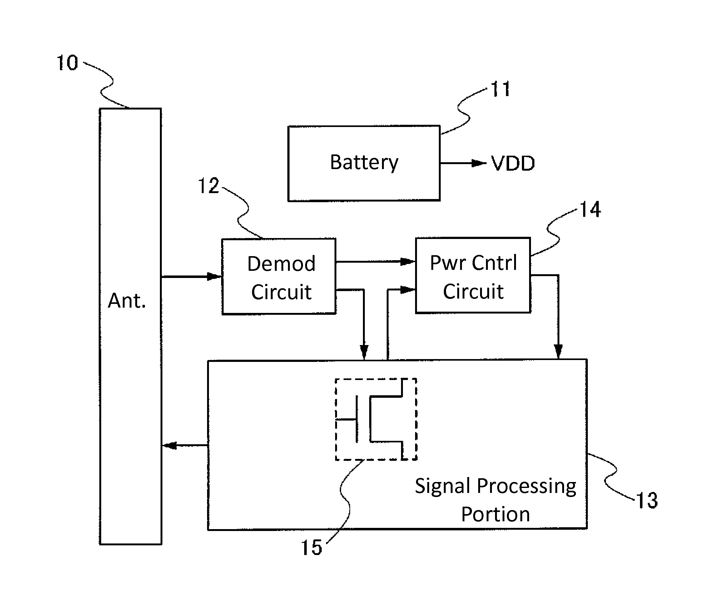
[0042]In this embodiment, an example of a semiconductor device will be described. Specifically, an example of a semiconductor device having a wireless communication function with a battery as a power supply source will be described with reference to FIG. 1.

[0043]A semiconductor device illustrated in FIG. 1 includes an antenna 10 capable of transmitting and receiving a wireless signal, a battery 11 serving as a supply source of power supply voltage (VDD), a demodulation circuit 12 demodulating a signal input from the antenna 10, a signal processing portion 13 operating with the use of a signal input from the demodulation circuit 12 and the power supply voltage (VDD) supplied from the battery 11, and a power control circuit 14 controlled by a signal input from the demodulation circuit 12 and a signal input from the signal processing portion 13. Note that in this embodiment, operation means generation of a signal in the signal processing portion 13 or part of the signal processing port...

embodiment 2

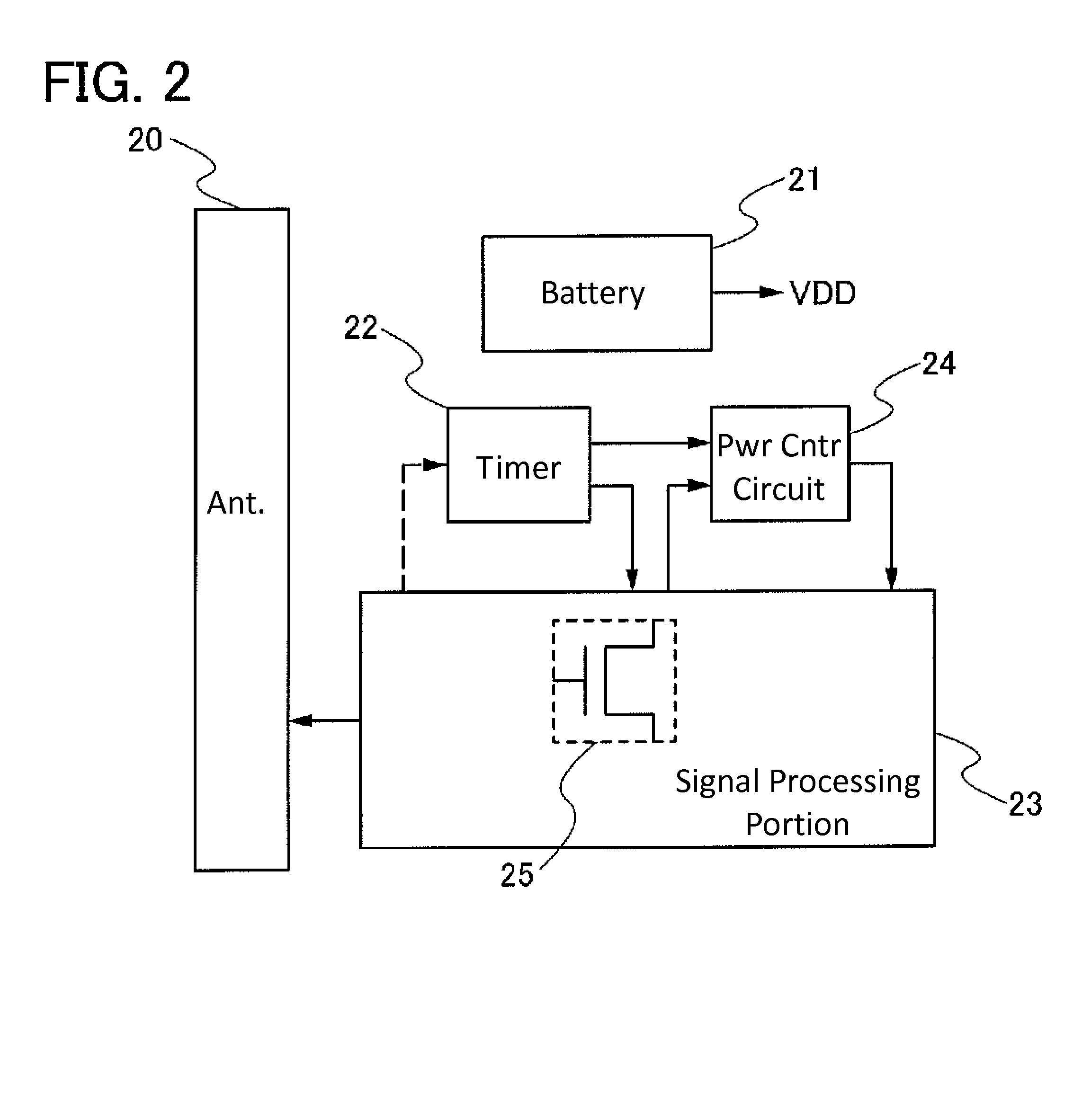
[0052]In this embodiment, an example of a semiconductor device will be described. Specifically, an example of a semiconductor device having a wireless communication function with a battery as a power supply source will be described with reference to FIG. 2.

[0053]A semiconductor device illustrated in FIG. 2 includes an antenna 20 capable of transmitting and receiving a wireless signal, a battery 21 serving as a supply source of power supply voltage (VDD), a timer 22 controlling intermittent operation of the semiconductor device by regularly outputting a signal, a signal processing portion 23 operating with the use of a signal input from the timer 22 and the power supply voltage (VDD) supplied from the battery 21, and a power control circuit 24 controlled by a signal input from the timer 22 and a signal input from the signal processing portion 23. Note that in this embodiment, operation means generation of a signal in the signal processing portion 23 or part of the signal processing p...

embodiment 3

[0061]In this embodiment, an example of a semiconductor device will be described. Specifically, an example of a semiconductor device having a wireless communication function with a secondary battery as a power supply source will be described with reference to FIG. 3.

[0062]A semiconductor device illustrated in FIG. 3 includes an antenna 30 capable of transmitting and receiving a wireless signal, a secondary battery 31 serving as a power supply source, a rectifier circuit 32 rectifying a signal input from the antenna 30, a charge circuit 33 charging the secondary battery 31 with the use of a signal input from the rectifier circuit 32, a stabilizing power supply circuit 34 generating power supply voltage (VDD) used in the semiconductor device with the use of the secondary battery 31, a demodulation circuit 35 demodulating a signal input from the antenna 30, a signal processing portion 36 operating with the use of a signal input from the demodulation circuit 35 and the power supply volt...


PUM


Abstract

An object is to achieve low power consumption and a long lifetime of a semiconductor device having a wireless communication function. The object can be achieved in such a manner that a battery serving as a power supply source and a specific circuit are electrically connected to each other through a transistor in which a channel formation region is formed using an oxide semiconductor. The hydrogen concentration of the oxide semiconductor is lower than or equal to 5×10¹⁹ (atoms / cm3). Therefore, leakage current of the transistor can be reduced. As a result, power consumption of the semiconductor device in a standby state can be reduced. Further, the semiconductor device can have a long lifetime.

Description

TECHNICAL FIELD[0001]The present invention relates to a semiconductor device, in particular, to a semiconductor device having a wireless communication function.[0002]Note that a semiconductor device in this specification refers to all electronic devices which can function by utilizing semiconductor characteristics, and electro-optical devices, semiconductor circuits, and electronic devices are all semiconductor devices.BACKGROUND ART[0003]Semiconductor devices having wireless communication functions for transmitting and receiving data wirelessly have been put into practical use in a variety of fields. Such semiconductor devices have been expected to further expand the market as a new mode of communication information terminals. In semiconductor devices having wireless communication functions, which are put into practical use, antennas and integrated circuits formed using semiconductor elements are formed over the same substrate. Further, semiconductor devices having wireless communi...

Claims


Application Information

Patent Timeline
Patent Type & Authority Patents(United States)
IPC IPC(8): H04B1/06H04B7/00H04B1/28H04M1/00G06K19/02G06K19/07G06K19/077G11C11/401H01L21/8234H01L27/088H01L29/786
CPCH01L27/0688H01L27/1225H01L29/7869H01L29/1033G06K19/07749H04B1/40Y02B60/50Y02D30/70Y02E60/10G06K19/07H01L29/06G06K19/07773H01L23/66H01L29/78696H01L2223/6677
Inventor KATO, KIYOSHIKOYAMA, JUN
Owner SEMICON ENERGY LAB CO LTD
Why Eureka
Try Eureka