Semiconductor device

a wireless communication and semiconductor technology, applied in secondary cells, electrochemical generators, instruments, etc., can solve the problems of unsuitable product management, long response time of wireless tags, and inability to supply constant electricity to tags, etc., to achieve high-speed operation of cpu systems, speed up memory operation, and reduce production costs

Active Publication Date: 2013-07-16
SEMICON ENERGY LAB CO LTD
View PDF44 Cites 1 Cited by
  • Summary
  • Abstract
  • Description
  • Claims
  • Application Information

AI Technical Summary

Benefits of technology

[0009]In order to speed up operation of the CPU system, an SRAM (static random access memory) which is capable of operating at high speed and does not need refreshing operation is favorable to be used as a cache memory even though the integration degree of the SRAM is lower than that of DRAM. Especially, by storing program data, which is often referred to in operation of the CPU, not in the DRAM but in the SRAM, reading time is shortened to speed up operation of systems.
[0012]In view of the foregoing problem, an object of the present invention is to allow rewriting of data in a memory included in the wireless tag provided with the CPU and speedup the CPU system so that communication performance of the wireless tag is improved.
[0013]The present invention provides a wireless power storage unit (RF battery) configured to store electricity transmitted wirelessly and an SRAM in a semiconductor device provided with a CPU. By supplying power from the wireless power storage unit to the SRAM, the semiconductor device with upgraded communication performance by speedup of the CPU system is provided. The SRAM is superior to other memories in a high reading and writing speed, in low power consumption during a waiting time, and in that a cycle time and an access time are the same. With the above-described features, the SRAM plays an important role for speedup of a system of the semiconductor device provided with the CPU. In addition, since the SRAM is combined with the wireless power storage unit, data in the SRAM can be stored and the SRAM has the same function as the ROM.
[0015]The semiconductor device of the present invention enables speedup of memory operation by providing an SRAM having a wireless power storage unit in order to use the SRAM as a program memory and / or a data memory, so that high-speed operation of a CPU system can be achieved. In addition, no data is stored in the SRAM which has been just manufactured so program data corresponding to application of the semiconductor device can be stored. Further, application of the semiconductor device is not limited in the manufacturing process so that production cost can be cut by mass production.

Problems solved by technology

However, unlike the PC, the wireless tag is not constantly supplied with electricity and the power supply often stops.
The wireless tag whose starting time is long and response is too slow is unsuitable for product management and the like.
Therefore, providing a system included in the above-described PC to the wireless tag is not practical.
This is because a tag which is moved at a speed higher than a certain value cannot be recognized, and that is one of the factors which limits an application of the wireless tag.

Method used


Image

  • Semiconductor device
  • Semiconductor device
  • Semiconductor device

Examples


embodiment mode 1

[Embodiment Mode 1]

[0028]When an SRAM provided with a wireless power storage unit is used as a memory for storing program data of a semiconductor device, program data can also be stored even when a power supply is off. Moreover, by using the SRAM, high-speed reading, writing, and erasing during memory access of a CPU can be achieved. Since writing and rewriting of program data is also possible, a semiconductor device provided with a CPU system in accordance with an application can be produced. Hereinafter, a structure and operation of the semiconductor device will be described.

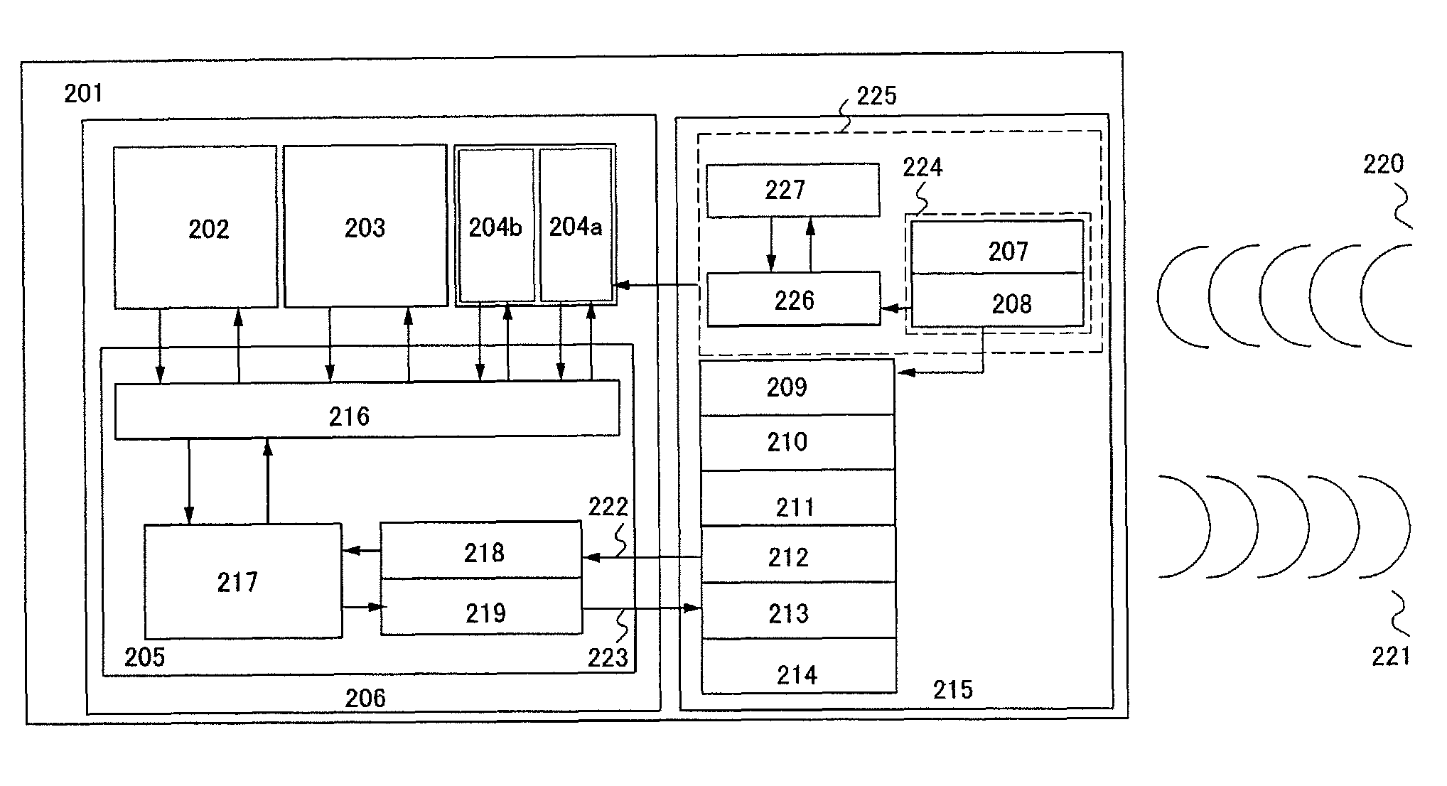
[0029]FIG. 1 illustrates a block diagram of the semiconductor device.

[0030]As shown in FIG. 1, a semiconductor device 201 includes a logic portion 206, and an analog portion 215. The logic portion 206 includes a CPU 202, a mask ROM 203, an SRAM 204a, an SRAM 204b, and a controller 205. The analog portion 215 includes a power supply circuit 209, a reset circuit 210, a clock generation circuit 211, a demodulatio...

embodiment mode 2

[Embodiment Mode 2]

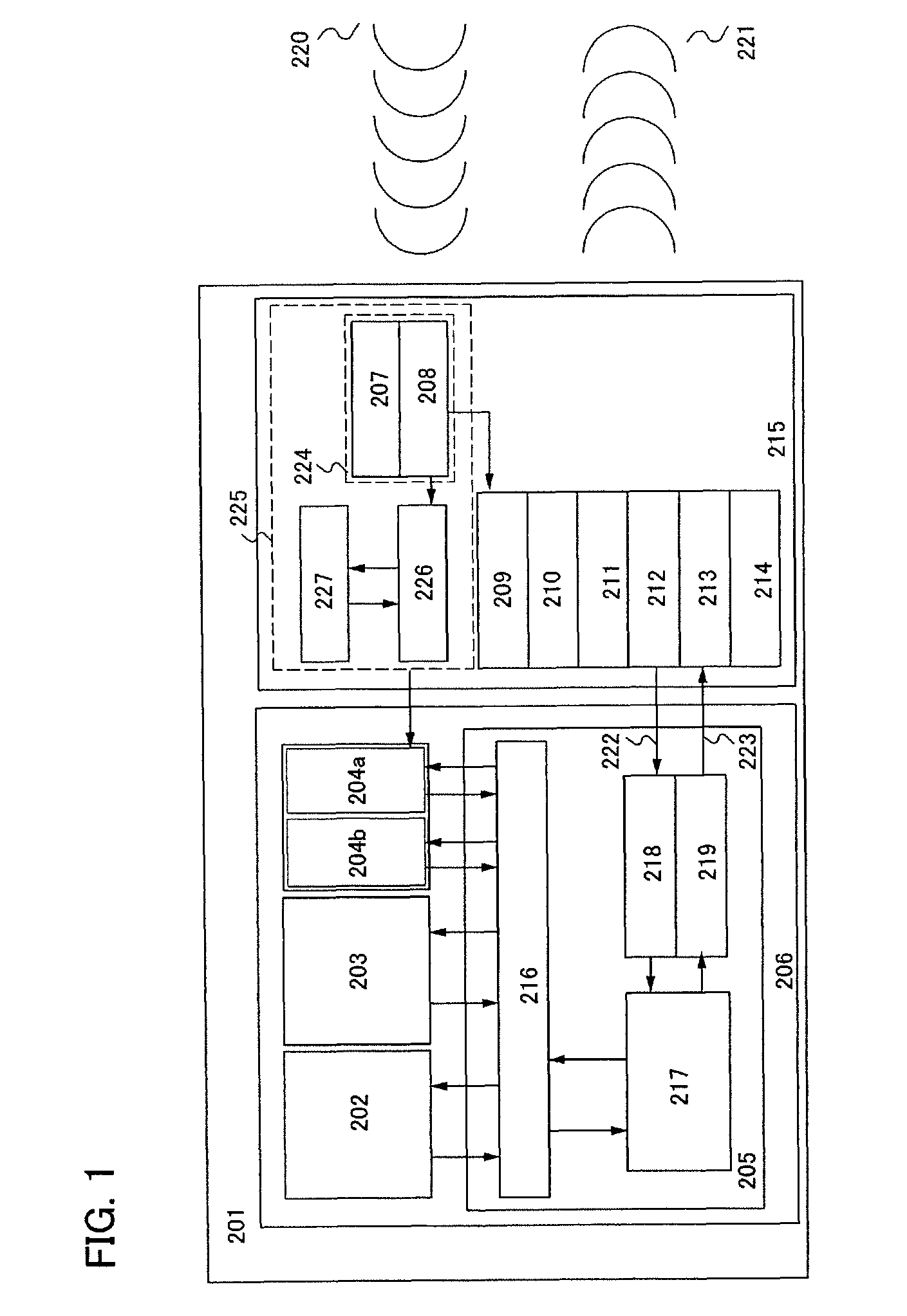
[0044]In this embodiment mode, a semiconductor device including a CPU and an SRAM provided with a wireless power storage unit will be described. FIG. 2 illustrates a block diagram of the semiconductor device in this embodiment mode.

[0045]The block structure of the semiconductor device will be described with reference to FIG. 2. In FIG. 2, a semiconductor device 101 includes a logic portion 106 and an analog portion 115. The logic portion 106 includes a CPU 102, a mask ROM 103, an SRAM 104, and a controller 105. The analog portion 115 includes a power supply circuit 109, a reset circuit 110, a clock generation circuit 111, a demodulation circuit 112, a modulation circuit 113, a power supply management circuit 114, and a wireless power storage unit 125. The wireless power storage unit 125 includes a antenna circuit 124, a power supply portion 126, and a power storage device 127. The antenna circuit 124 includes an antenna 107 and a resonance circuit 108.

[0046]The co...

embodiment mode 3

[Embodiment Mode 3]

[0058]Next, an exemplary structure of a semiconductor device 800 will be described with reference to FIG. 3. FIG. 3 is a block diagram of the semiconductor device 800. The semiconductor device 800 includes an antenna circuit 801, a signal processing circuit 802, and a power storage device 803.

[0059]The antenna circuit 801 transmits and receives signals. The antenna circuit 801 detects signals whose frequency corresponds to a form of the antenna circuit. A signal received by the antenna circuit 801 is converted into a DC power supply by the signal processing circuit 802 so that electricity is supplied to the power storage device 803.

[0060]A so-called storage battery (battery) can be applied to the power storage device 803. For example, a secondary battery such as a lithium-ion battery, a lithium secondary battery, a nickel hydride battery, a nickel-cadmium battery, an organic radical battery, a lead storage battery, an air secondary battery, a nickel-zinc battery, ...


PUM


Abstract

Communication performance of the wireless tag is improved by providing an SRAM provided with an RF battery in the wireless tag provided with a CPU to speed up the CPU system. Moreover, rewriting of data in a memory of a wireless tag provided with a CPU is enabled. An RF battery includes an antenna circuit, a power supply portion, and a power storage device. A function as a non-volatile memory is provided to an SRAM by combining the SRAM and an RF battery.

Description

BACKGROUND OF THE INVENTION[0001]1. Field of the Invention[0002]The present invention relates to a semiconductor device for wireless communication. In particular, the present invention relates to a semiconductor device for wireless communication provided with a CPU (central processing unit).[0003]2. Description of the Related Art[0004]Recently a small-sized semiconductor device (a wireless tag) combining an ultra small IC chip and an antenna circuit for wireless communication has attracted a lot of attention. The wireless tag can read and write data by transmitting and receiving communication signals, with a wireless communication device (hereinafter referred to as a reader / writer). Although the wireless tag often has a card form or a chip form which is much smaller than the card form, it may have various forms depending on use.[0005]As a field of application of the wireless tag, for example, product management in distribution industry is an example. These days product management wi...

Claims


Application Information

Patent Timeline
Patent Type & Authority Patents(United States)
IPC IPC(8): H04Q5/22G06K19/07H01L21/8244H01L21/8246H01L27/11H01L27/112
CPCH01M10/425H01M10/46H01M10/44Y02E60/10
Inventor KOZUMA, MUNEHIROKUROKAWA, YOSHIYUKI
Owner SEMICON ENERGY LAB CO LTD
Why Eureka
Try Eureka