Lead frame ball grid array with traces under die
a grid array and lead frame technology, applied in the field of semiconductor packaging, can solve the problems of unreliable ic packages, unwieldy additional step of mounting standoffs, unreliable, etc., and achieve the effect of enhancing reliability, and increasing the standoff height of the devi
- Summary
- Abstract
- Description
- Claims
- Application Information
AI Technical Summary
Benefits of technology
Problems solved by technology
Method used
Image

Examples
Embodiment Construction
[0071]In the following description, numerous details and alternatives are set forth for purpose of explanation. However, one of ordinary skill in the art having the benefit of this disclosure will realize that the invention can be practiced without the use of these specific details. In other instances, well-known structures and devices are shown in block diagram form in order not to obscure the description of the invention with unnecessary detail.
I. Method
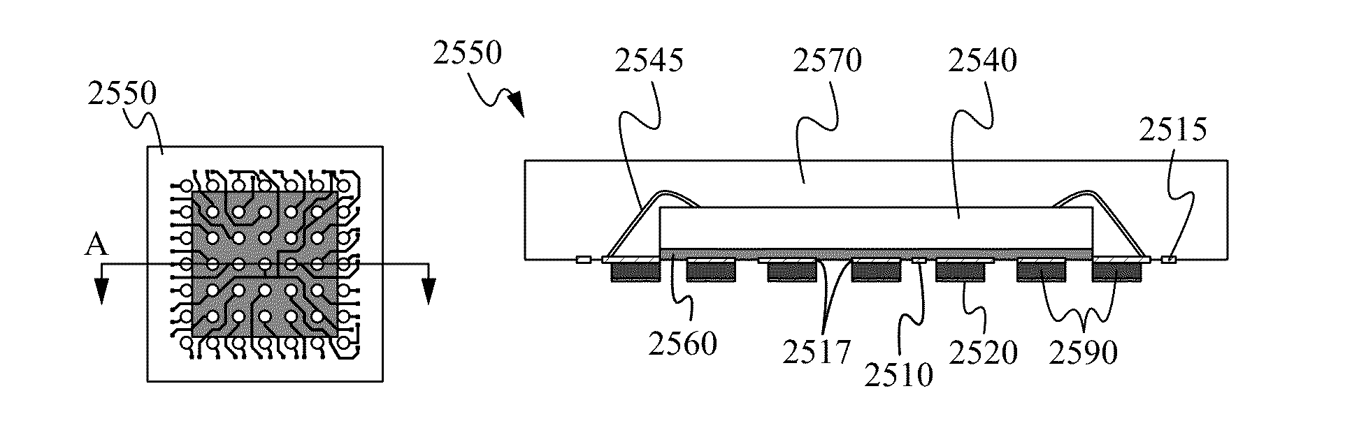
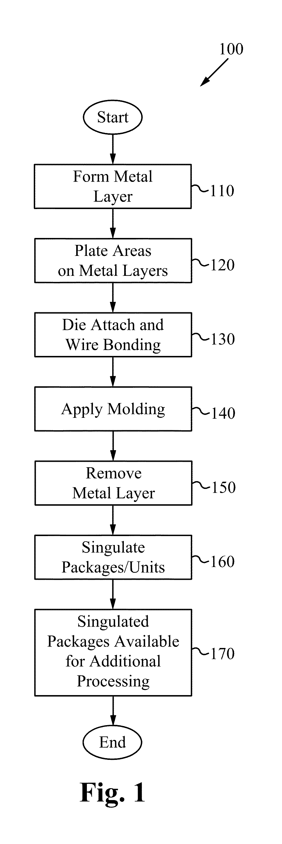
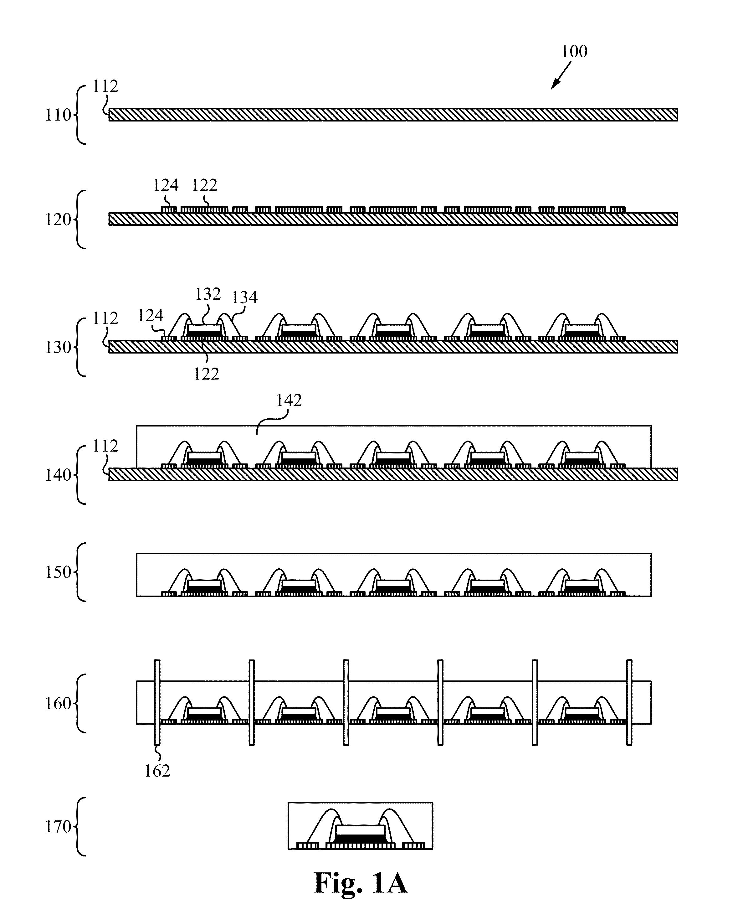
[0072]FIG. 1 illustrates a process 100 for manufacturing a semiconductor package according to some embodiments of the invention. FIG. 1A illustrates an exemplary result for each step in the process 100 of FIG. 1. As shown in these figures, the process 100 begins at the step 110, where a metal layer 112 is formed. The metal layer typically comprises copper, Alloy 42, or another suitable metal material, and has a typical thickness of about 0.1 to 0.15 millimeters. Then, after the step 110, the process 100 transitions to the step 120,...
PUM
 Abstract
Description
Claims
Application Information