Organic laser device
a laser device and organic technology, applied in the field of laser devices, can solve problems such as large number of problems
- Summary
- Abstract
- Description
- Claims
- Application Information
AI Technical Summary
Benefits of technology
Problems solved by technology
Method used
Image
Examples
embodiment 1
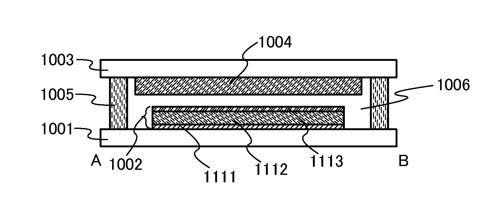
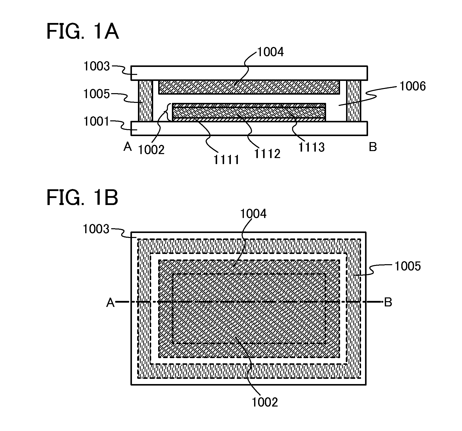
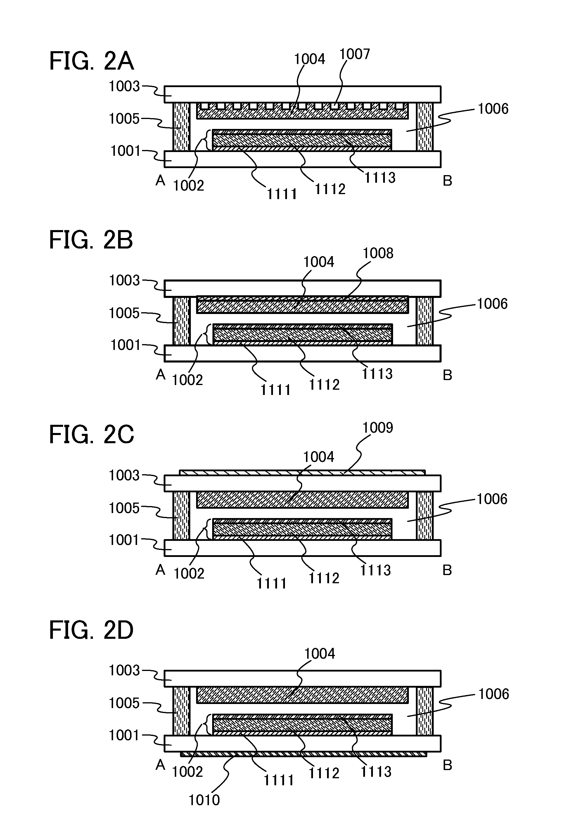
[0035]An organic laser device of this embodiment is a laser device with which a laser medium and a light source are integrated. A light-emitting element is used as the light source. The light-emitting element is a plane light source. Further, a film containing a laser dye as a laser medium is formed in a region facing the light source. An optical resonator is preferably provided with a substrate over which the film containing a laser dye as a laser medium is formed. The arrangement of the optical resonator over the laser medium is not particularly limited. The optical resonator may be provided inside the laser medium, on a substrate side of the laser medium, or on a surface side of the laser medium.
[0036]A laser device having such a structure emits laser light by excitation of a laser dye as a laser medium by light from a light-emitting element.
[0037]In addition, a substrate over which a light-emitting element is formed and a substrate over which a laser medium is formed are placed ...
embodiment 2
[0071]In this embodiment, one embodiment of the light-emitting element will be described with reference to FIGS. 3A and 3B.
[0072]The light-emitting element of this embodiment has a plurality of layers between a pair of electrodes. The plurality of layers has a light-emitting region which is formed apart from the electrodes. That is, the plurality of layers is stacked by combining layers made of a substance having a high carrier-injecting property and a substance having a high carrier-transporting property so that carriers are recombined at a position away from the electrodes.
[0073]In this embodiment, the light-emitting element includes a first electrode 102, a second electrode 104, and an EL layer 103 provided between the first electrode 102 and the second electrode 104. Note that in the following description of this embodiment, it is assumed that the first electrode 102 functions as an anode and the second electrode 104 functions as a cathode. In other words, it is assumed when a v...
embodiment 3
[0107]In this embodiment, one embodiment of a light-emitting element will be described in detail with reference to FIG. 4. In this embodiment, a light-emitting element having a structure in which a plurality of light-emitting units is stacked (hereinafter, referred to as a stacked-type element) will be described. This light-emitting element is a stacked-type light-emitting element having a plurality of light-emitting units between a first electrode and a second electrode. Each light-emitting unit can have a similar structure to the structure of the EL layer described in Embodiment 2. In other words, the light-emitting element described in Embodiment 2 is a light-emitting element having one light-emitting unit. In this embodiment, a light-emitting element having a plurality of light-emitting units will be described.
[0108]In FIG. 4, between a first electrode 501 and a second electrode 502, a first light-emitting unit 511 and a second light-emitting unit 512 are stacked with a charge-g...
PUM
 Abstract
Description
Claims
Application Information


