High quality GaN high-voltage HFETS on silicon

a technology of high-voltage hfets and silicon, which is applied in the direction of semiconductor devices, electrical equipment, transistors, etc., can solve the problems of poor thermal conductors, limited application of gan-based devices to specific markets, and the cost of sic wafers remains high

Active Publication Date: 2013-08-13
POWER INTEGRATIONS INC
View PDF2 Cites 12 Cited by
  • Summary
  • Abstract
  • Description
  • Claims
  • Application Information

AI Technical Summary

Problems solved by technology

However, the difficulty and expense in forming GaN substrates have limited the application of GaN-based devices to specific markets.
A GaN substrate is typically manufactured by growing GaN film on another substrate, due to the expense and difficulty of manufacturing bulk GaN wafers.
However, sapphire is a poor thermal conductor and can present difficulties during packaging, and SiC wafers are still very expensive.
Moreover, both types of wafers are only available as smaller-diameter wafers, which eliminate the economy of scales available with larger diameters.
However, due to a large lattice mismatch and large thermal mismatch between GaN and silicon, it may be difficult to reliably grow GaN directly on a silicon (Si) substrate.

Method used


Image

  • High quality GaN high-voltage HFETS on silicon
  • High quality GaN high-voltage HFETS on silicon
  • High quality GaN high-voltage HFETS on silicon

Examples


Embodiment Construction

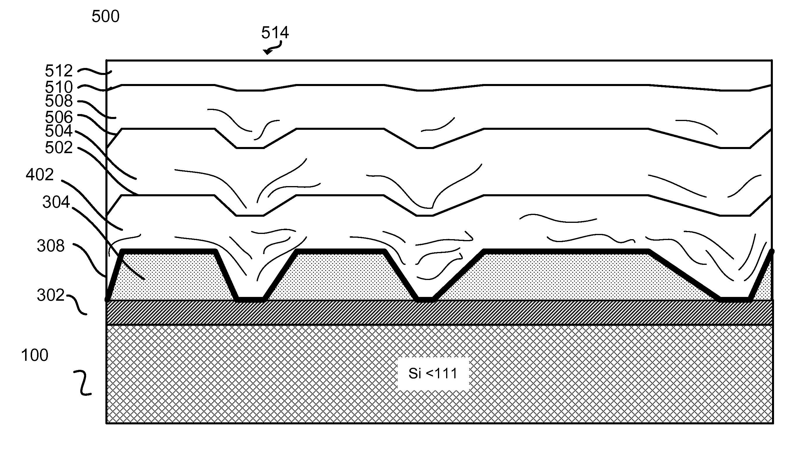
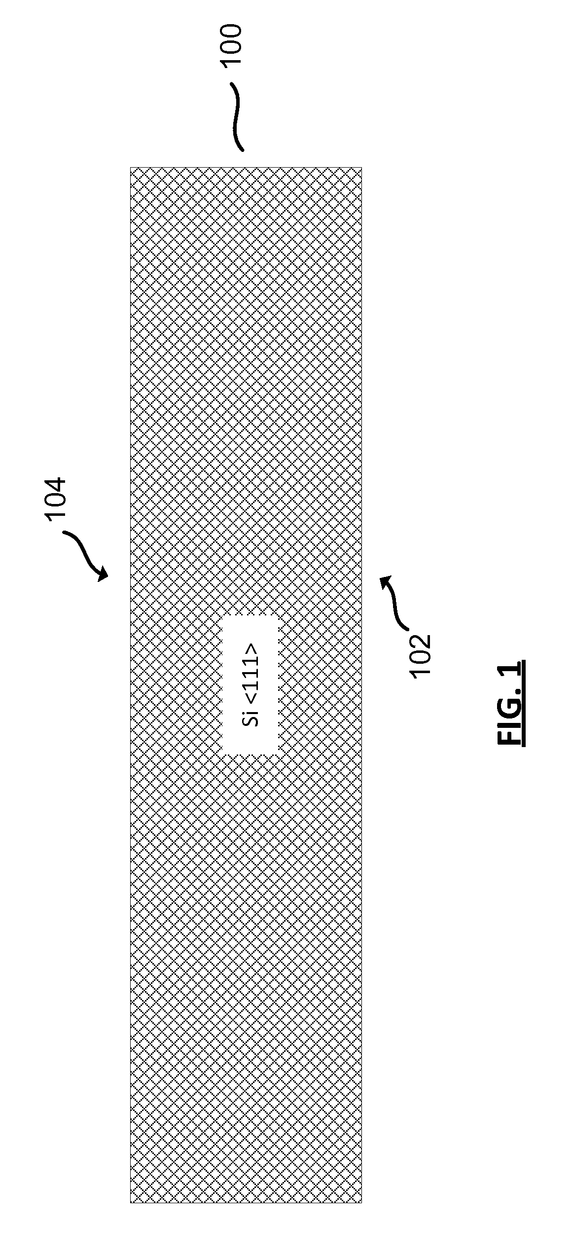
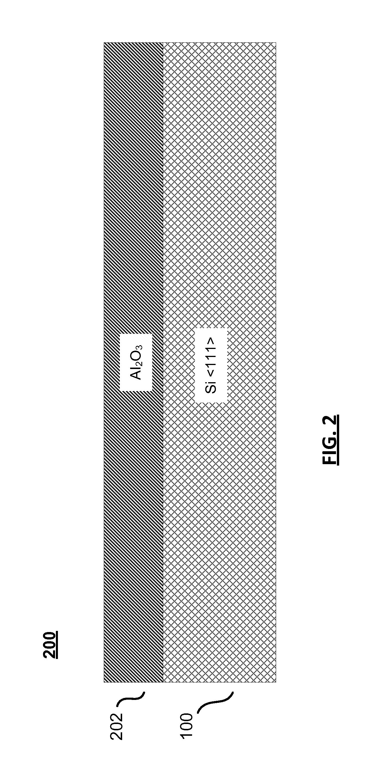
[0016]In the following description, numerous specific details are set forth in order to provide a thorough understanding of the present invention. It will be apparent, however, to one having ordinary skill in the art that the specific detail need not be employed to practice the present invention. In other instances, well-known materials or methods have not been described in detail in order to avoid obscuring the present invention.

[0017]Reference throughout this specification to “one embodiment”, “an embodiment”, “one example” or “an example” means that a particular feature, structure or characteristic described in connection with the embodiment or example is included in at least one embodiment of the present invention. Thus, appearances of the phrases “in one embodiment”, “in an embodiment”, “one example” or “an example” in various places throughout this specification are not necessarily all referring to the same embodiment or example. Furthermore, the particular features, structure...


PUM


Abstract

Substrates of GaN over silicon suitable for forming electronics devices such as heterostructure field effect transistors (HFETs), and methods of making the substrates, are disclosed. Voids in a crystalline Al2O3 film on a top surface of a silicon wafer are formed. The top surface of the silicon wafer is along the <111> silicon crystal orientation. A plurality of laminate layers is deposited over the voids and the Al2O3 film. Each laminate layer includes an AlN film and a GaN film. A transistor or other device may be formed in the top GaN film.

Description

BACKGROUND[0001]1. Field[0002]The present disclosure relates generally to gallium nitride (GaN) substrates, and, more specifically, the present disclosure relates to a method for fabricating a GaN substrate on silicon.[0003]2. Description of Related Art[0004]Wide-bandgap semiconductors are widely used for fabricating active devices for high-voltage applications. One type of semiconductor structure known as a heterostructure field effect transistors (HFET) (also called high-electron mobility transistors (HEMT)) uses wide-bandgap semiconductors to implement transistors for high-performance power electronics. In one example, wide-bandgap HFET devices may be used as a switching element in high-voltage switching power converters.[0005]GaN is one example of a wide-bandgap semiconductor that has generated particular interest. For example, AlGaN / GaN HFETs show promise for power electronics due to their wider bandgap and high-electron saturation velocity, both of which enable high-voltage op...

Claims


Application Information

Patent Timeline
Patent Type & Authority Patents(United States)
IPC IPC(8): H01L31/072
CPCH01L21/02642H01L21/0262H01L21/0226H01L21/02381H01L21/02458H01L29/2003H01L29/205H01L29/78H01L21/0254H01L29/7786H01L29/1075H01L21/02488H01L29/045H01L29/778
Inventor RAMDANI, JAMALEDWARDS, JOHN P.LIU, LINLIN
Owner POWER INTEGRATIONS INC
Why Eureka
Try Eureka