Methods for the fabrication of integrated circuits including back-etching of raised conductive structures

a technology of raised conductive structures and integrated circuits, which is applied in the direction of basic electric elements, electrical equipment, semiconductor devices, etc., to achieve the effect of reducing parasitic fringing capacitance and increasing the width of the lateral gap

Active Publication Date: 2013-09-03
GLOBALFOUNDRIES U S INC
View PDF3 Cites 7 Cited by
  • Summary
  • Abstract
  • Description
  • Claims
  • Application Information

AI Technical Summary

Benefits of technology

[0006]Embodiments of a method for fabricating an integrated circuit are provided. In one embodiment, the method includes producing a partially-completed semiconductor device including a substrate, source / drain (S / D) regions, a channel region between the S / D regions, and a gate stack over the channel region. At least one raised electrically-conductive structure is formed over at least one of the S / D regions and separated from the gate stack by a lateral gap. The raised electrically-conductive structure is then back-etched to increase the width of the lateral gap and reduce the parasitic fringing capacitance between the raised electrically-conductive structure and the gate stack during operation of the completed semiconductor device.

Problems solved by technology

Such parasitic fringing capacitances can significantly delay the switching speed of PMOS transistor 20 and are consequently undesirable.

Method used


Image

  • Methods for the fabrication of integrated circuits including back-etching of raised conductive structures
  • Methods for the fabrication of integrated circuits including back-etching of raised conductive structures
  • Methods for the fabrication of integrated circuits including back-etching of raised conductive structures

Examples


Embodiment Construction

[0012]The following Detailed Description is merely exemplary in nature and is not intended to limit the invention or the application and uses of the invention. Furthermore, there is no intention to be bound by any expressed or implied theory presented in the preceding Technical Field, Background, Brief Summary, or the following Detailed Description.

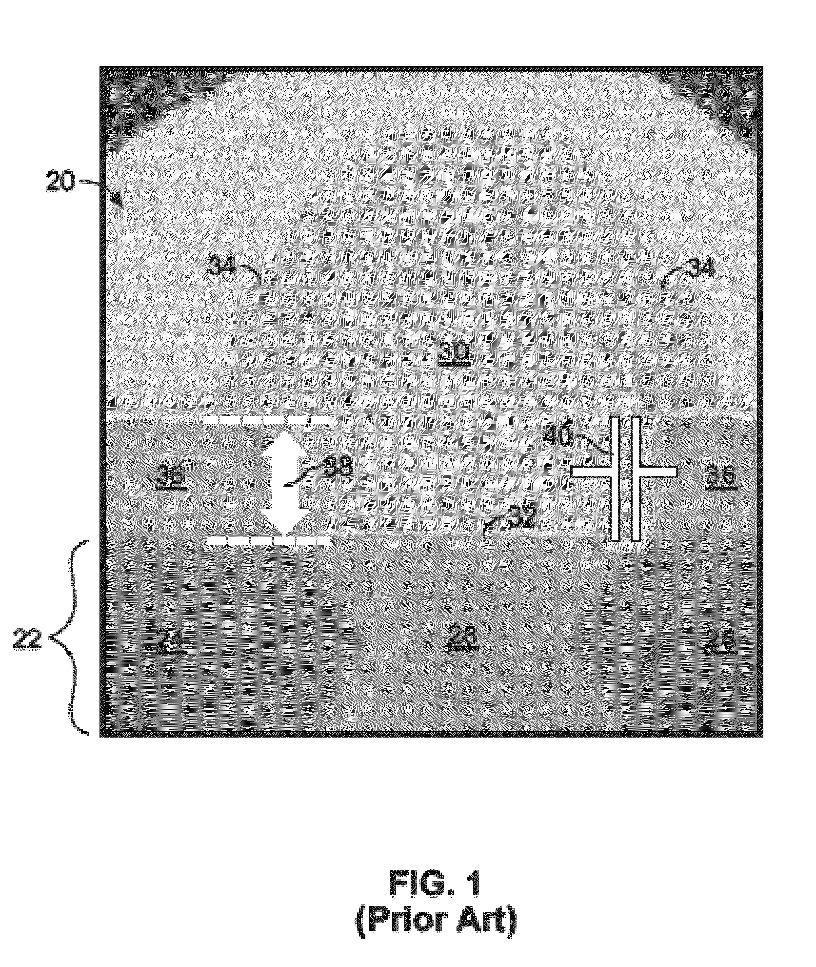
[0013]FIG. 1 is a transmission electron microscope (TEM) image of a PMOS transistor 20 illustrated in accordance with the teachings of prior art. PMOS transistor 20 includes a semiconductor substrate 22; S / D regions 24, 26 within substrate 22; and a channel region 28 extending between S / D regions 24, 26. A gate 30 is formed over channel region 28 and electrically isolated therefrom by an intervening dielectric layer 32. Sidewall spacers 34 are formed laterally adjacent opposing sides of gate 30. As indicated in FIG. 1 by the shape of the interface between channel 28 and S / D regions 24, 26, a strain material has been embedded into S / D regi...


PUM


Abstract

Embodiments of a method for fabricating an integrated circuit are provided. In one embodiment, the method includes producing a partially-completed semiconductor device including a substrate, source / drain (S / D) regions, a channel region between the S / D regions, and a gate stack over the channel region. At least one raised electrically-conductive structure is formed over at least one of the S / D regions and separated from the gate stack by a lateral gap. The raised electrically-conductive structure is then back-etched to increase the width of the lateral gap and reduce the parasitic fringing capacitance between the raised electrically-conductive structure and the gate stack during operation of the completed semiconductor device.

Description

TECHNICAL FIELD[0001]The present invention relates generally to integrated circuits and, more particularly, to methods for the fabrication of integrated circuits wherein raised-conductive structures adjacent the transistor gates are back-etched to reduce parasitic fringing capacitances.BACKGROUND[0002]Although technically referring to a semiconductor device having a metal gate electrode and an oxide gate insulator, the term “MOS transistor” is now commonly utilized (and is utilized herein) to refer to any semiconductor device including a conductive gate electrode (whether metal or other conductive material) positioned over a gate insulator (whether oxide or other insulator), which is, in turn, positioned over a semiconductor substrate. The gain of a MOS transistor, usually defined by the transconductance (gm), is proportional to the mobility (μ) of the majority carrier in the transistor channel. The current carrying capacity, and hence the performance of a MOS transistor, is proport...

Claims


Application Information

Patent Timeline
Patent Type & Authority Patents(United States)
IPC IPC(8): H01L21/336
CPCH01L21/84H01L21/823425H01L21/823412
Inventor FLACHOWSKY, STEFANMIKALO, RICARDO P.HOENTSCHEL, JAN
Owner GLOBALFOUNDRIES U S INC
Why Eureka
Try Eureka