

Method for fabricating super-junction power device with reduced miller capacitance
a super-junction semiconductor and miller capacitance technology, applied in the direction of semiconductor devices, basic electric elements, electrical appliances, etc., can solve the problems of reducing the performance of the device, the channel length is not easily controlled, and the threshold voltage fluctuation, so as to reduce the miller capacitance and simplify the processing steps
- Summary
- Abstract
- Description
- Claims
- Application Information
AI Technical Summary
Benefits of technology
Problems solved by technology
Method used
Image

Examples
Embodiment Construction
[0015]In the following description, numerous specific details are given to provide a thorough understanding of the invention. It will, however, be apparent to one skilled in the art that the invention may be practiced without these specific details. Furthermore, some well-known system configurations and process steps are not disclosed in detail, as these should be well-known to those skilled in the art.
[0016]Likewise, the drawings showing embodiments of the apparatus are semi-diagrammatic and not to scale, and some dimensions are exaggerated in the figures for clarity of presentation. Also, where multiple embodiments are disclosed and described as having some features in common, like or similar features will usually be described with like reference numerals for ease of illustration and description thereof.
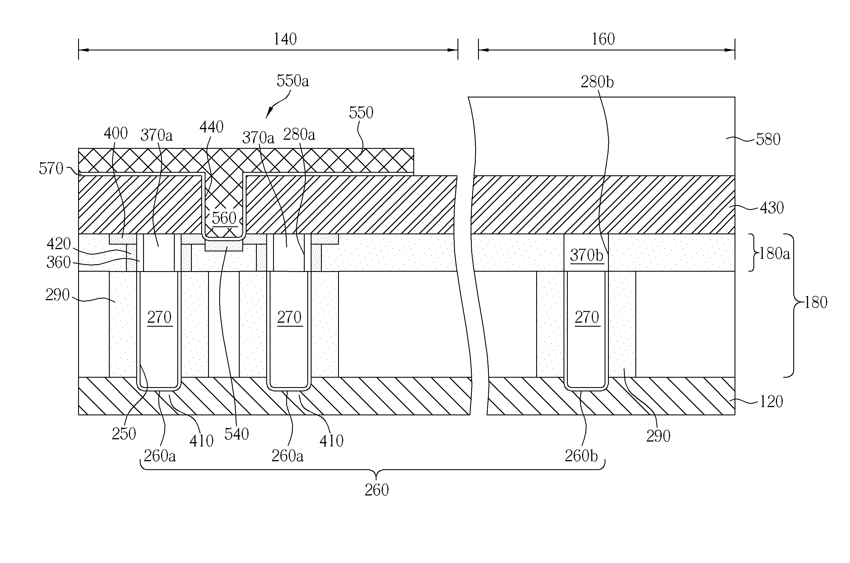
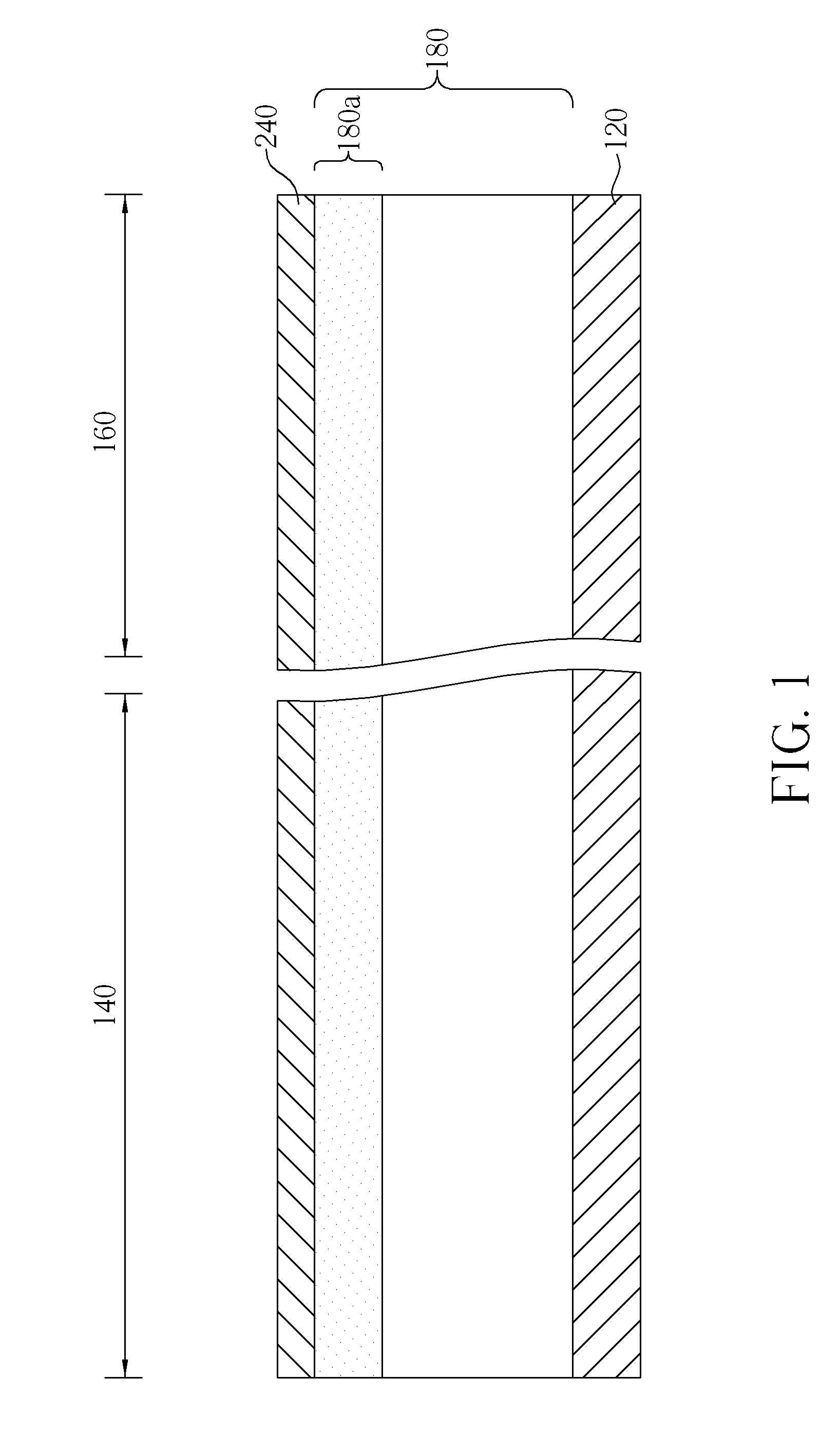
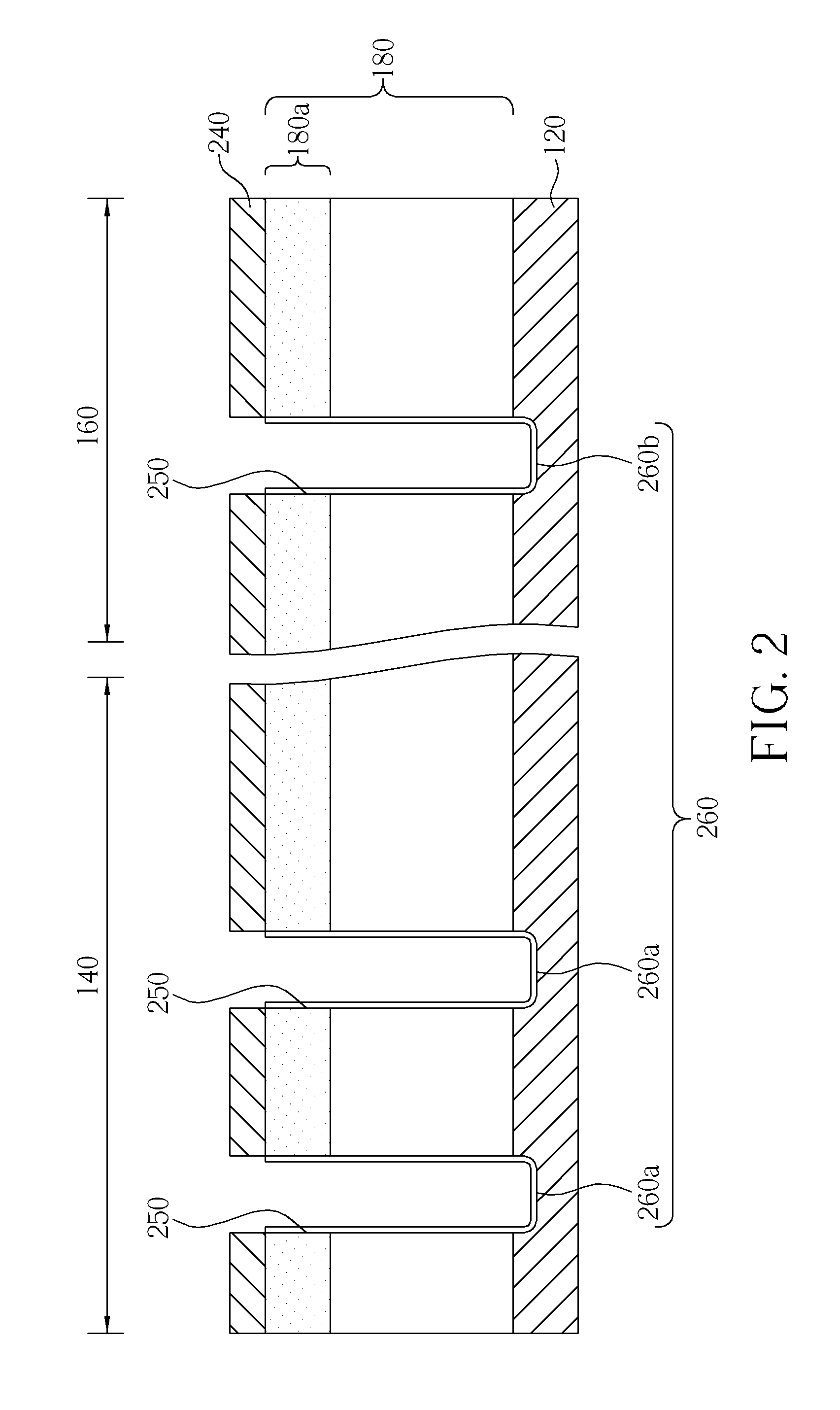
[0017]FIGS. 1-8 are schematic, cross-sectional diagrams showing a method for fabricating a super-junction power device with reduced Miller capacitance according to one embodiment o...
PUM
 Abstract
Description
Claims
Application Information