Trench isolation MOS P-N junction diode device and method for manufacturing the same
a technology of mos and mos, which is applied in the direction of semiconductor devices, electrical equipment, transistors, etc., can solve the problems of -n junction diodes having a forward voltage drop higher, schottky diodes have relatively low reverse voltage tolerance, and the reverse recovery time is longer, so as to simplify the naming of the device, the effect of low forward voltage drop and rapid switching speed
- Summary
- Abstract
- Description
- Claims
- Application Information
AI Technical Summary
Benefits of technology
Problems solved by technology
Method used
Image
Examples
first embodiment
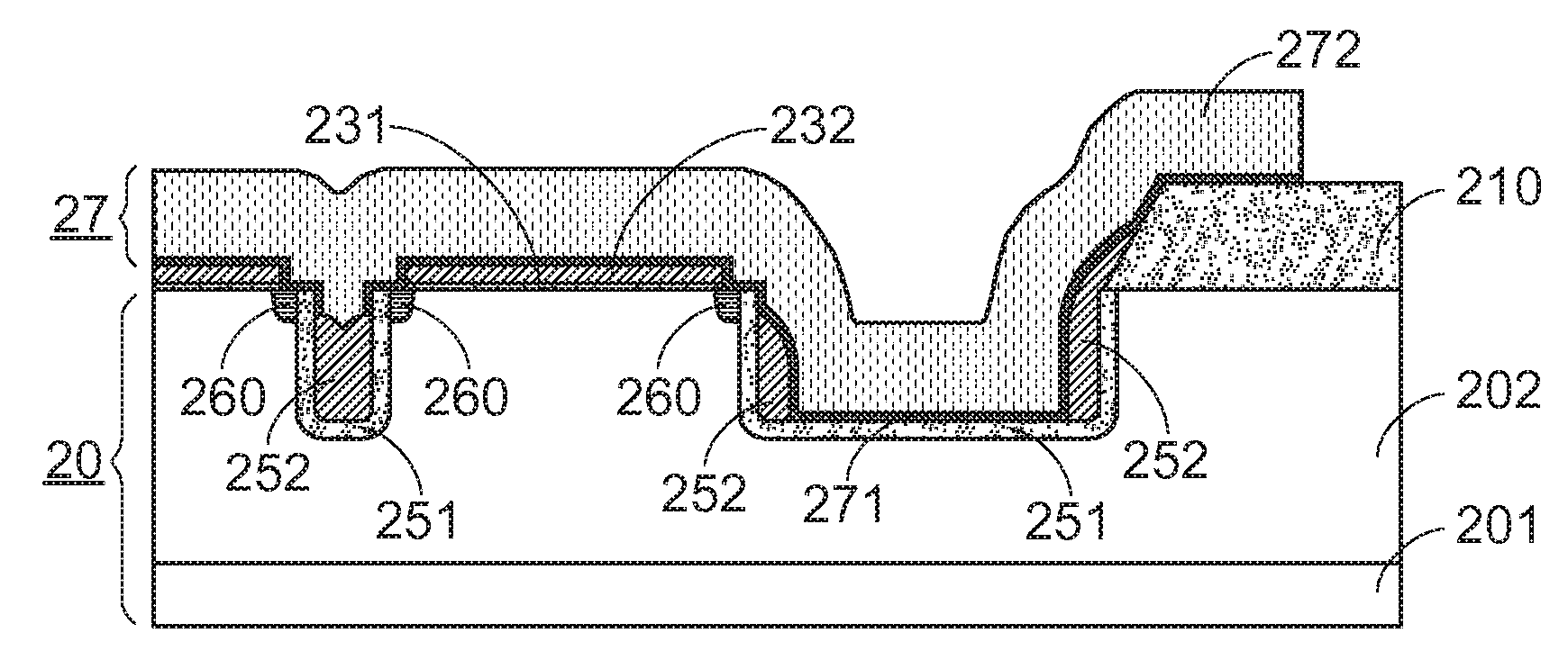
[0017]Please refer to FIGS. 2A˜2R, which schematically illustrate a method of manufacturing a trench isolation metal-oxide-semiconductor (MOS) P-N junction diode device (i-MOS Rectifier) according to the present invention.
[0018]Firstly, as shown in FIG. 2A, a substrate 20 with a heavily-doped N-type silicon layer 201 (N+ silicon layer) and a lightly-doped N-type epitaxial layer 202 (N− epitaxial layer) is provided. Then, as shown in FIG. 2B, a first mask layer 210 (an oxide layer) is grown on the substrate 20 by thermal oxidation. Then, a photoresist layer 211 is formed on the first mask layer 210 (FIG. 2C). A first photolithography process is performed to define a patterned photoresist zone 2111 and a photoresist-free zone 2110 of the photoresist layer 211 (FIG. 2D). An etching process is performed to remove the first mask layer 210 uncovered by the patterned photoresist zone 2111. After the remaining patterned photoresist zone 2111 is removed, a sidewall structure 22 is formed on ...
second embodiment
[0023]Please refer to FIGS. 3A-3R, which schematically illustrate a method of manufacturing a trench isolation metal-oxide-semiconductor (MOS) P-N junction diode device (i-MOS Rectifier) according to the present invention.
[0024]Firstly, as shown in FIG. 3A, a substrate 30 with a heavily-doped N-type silicon layer 301 (N+ silicon layer) and a lightly-doped N-type epitaxial layer (N− epitaxial layer) 302 is provided. Then, as shown in FIG. 3B, a first mask layer 310 (an oxide layer) is grown on the substrate 30 by thermal oxidation. Then, a photoresist layer 311 is formed on the first mask layer 310 (FIG. 3C). Then, a first photolithography process is performed to define a patterned photoresist zone 3111 and a photoresist-free zone 3110 of the photoresist layer 311 (FIG. 3D). A dry etching process is performed to remove the first mask layer 310 uncovered by the patterned photoresist zone 3111 to form a concave structure 40 in the first mask layer 310. Then, the remaining patterned pho...
PUM
 Abstract
Description
Claims
Application Information


