Trench isolation mos p-n junction diode device and method for manufacturing the same

a technology of mos and mos, which is applied in the direction of semiconductor devices, electrical equipment, transistors, etc., can solve the problems of -n junction diodes having a forward voltage drop higher, schottky diodes have relatively low reverse voltage tolerance, and the reverse recovery time is longer, so as to simplify the naming of the device, the effect of low forward voltage drop and rapid switching speed

Active Publication Date: 2012-03-01
PFC DEVICE HLDG
View PDF9 Cites 14 Cited by
  • Summary
  • Abstract
  • Description
  • Claims
  • Application Information

AI Technical Summary

Benefits of technology

[0008]Therefore, the present invention relates to a trench isolation metal-oxide-semiconductor (MOS) P-N junction diode device and a manufacturing method thereof. To simplify the naming for this device, it is also named as Isolated MOS Rectifier (i-MOS Rectifier). The trench isolation MOS P-N junction diode device is a combination of an N-channel MOS structure and a lateral P-N junction diode, wherein a poly-silicon-filled trench oxide layer is buried in the P-type structure to replace the majority of the P-type structure. In a forward mode, the N-channel MOS structure and the P-N junction diode (i-MOS Rectifier) are connected with each other in parallel. Under this circumstance, like the Schottky diode, the trench isolation MOS P-N junction diode device (i-MOS Rectifier) has low forward voltage drop and rapid switching speed. Whereas, in a reverse mode, the leakage current is pinched off and the N-channel is shut off by the poly-silicon—filled trench oxide layer and the depletion region of the lateral P-N junction diode, so that the trench isolation MOS P-N junction diode device (i-MOS Rectifier) has low leakage current. In addition, since the poly-silicon-filled trench oxide layer is buried in the P-type structure to replace the majority of the P-type structure, the area of the P-type structure is reduced and the influence of the carrier effect is reduced. Under this circumstance, the trench isolation MOS P-N junction diode device has shorter reverse recovery time. As a result, the trench isolation MOS P-N junction diode device of the present invention has the benefits of the Schottky diode and the P-N junction diode. That is, the trench isolation MOS P-N junction diode device (i-MOS Rectifier) of the present invention has rapid switching speed, low forward voltage drop, low reverse leakage current and short reverse recovery time.

Problems solved by technology

The limitations of Schottky diodes are the relatively low reverse voltage tolerance and the relatively high reverse leakage current.
The limitations are related to the Schottky barrier determined by the metal work function of the metal electrode, the band gap of the intrinsic semiconductor, the type and concentration of dopants in the semiconductor layer, and other factors.
However, the P-N junction diode has a forward voltage drop higher than that of the Schottky diode, and takes longer reverse recovery time due to a slow and random recombination of electrons and holes during the recovery period.

Method used


Image

  • Trench isolation mos p-n junction diode device and method for manufacturing the same
  • Trench isolation mos p-n junction diode device and method for manufacturing the same
  • Trench isolation mos p-n junction diode device and method for manufacturing the same

Examples


first embodiment

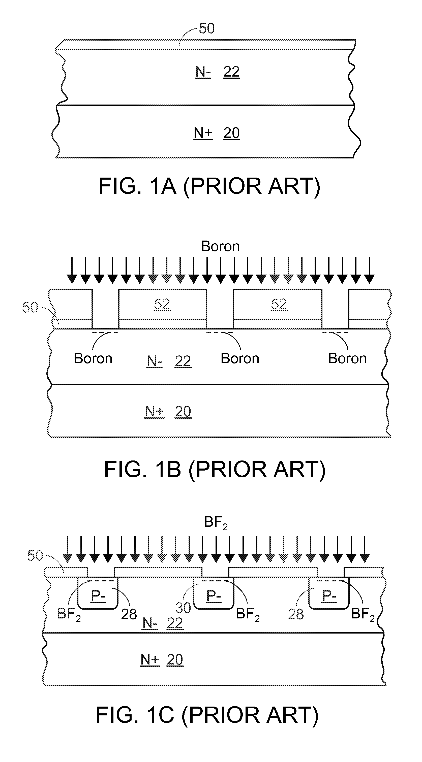
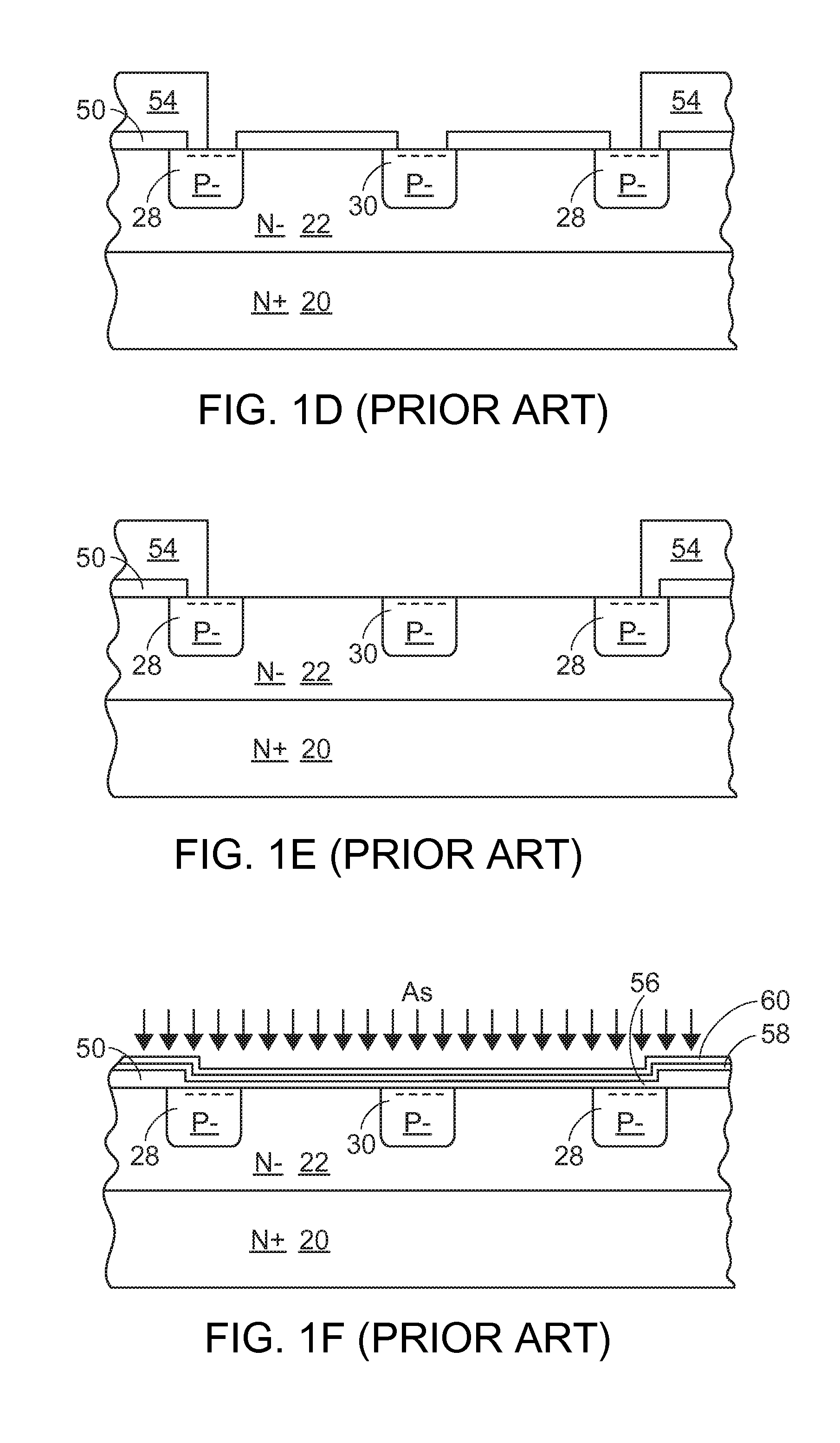
[0017]Please refer to FIGS. 2A˜2R, which schematically illustrate a method of manufacturing a trench isolation metal-oxide-semiconductor (MOS) P-N junction diode device (i-MOS Rectifier) according to the present invention.

[0018]Firstly, as shown in FIG. 2A, a substrate 20 with a heavily-doped N-type silicon layer 201 (N+ silicon layer) and a lightly-doped N-type epitaxial layer 202 (N− epitaxial layer) is provided. Then, as shown in FIG. 2B, a first mask layer 210 (an oxide layer) is grown on the substrate 20 by thermal oxidation. Then, a photoresist layer 211 is formed on the first mask layer 210 (FIG. 2C). A first photolithography process is performed to define a patterned photoresist zone 2111 and a photoresist-free zone 2110 of the photoresist layer 211 (FIG. 2D). An etching process is performed to remove the first mask layer 210 uncovered by the patterned photoresist zone 2111. After the remaining patterned photoresist zone 2111 is removed, a sidewall structure 22 is formed on ...

second embodiment

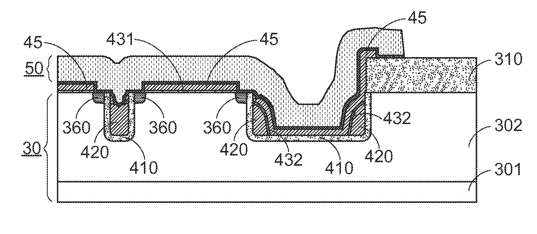
[0023]Please refer to FIGS. 3A-3R, which schematically illustrate a method of manufacturing a trench isolation metal-oxide-semiconductor (MOS) P-N junction diode device (i-MOS Rectifier) according to the present invention.

[0024]Firstly, as shown in FIG. 3A, a substrate 30 with a heavily-doped N-type silicon layer 301 (N+ silicon layer) and a lightly-doped N-type epitaxial layer (N− epitaxial layer) 302 is provided. Then, as shown in FIG. 3B, a first mask layer 310 (an oxide layer) is grown on the substrate 30 by thermal oxidation. Then, a photoresist layer 311 is formed on the first mask layer 310 (FIG. 3C). Then, a first photolithography process is performed to define a patterned photoresist zone 3111 and a photoresist-free zone 3110 of the photoresist layer 311 (FIG. 3D). A dry etching process is performed to remove the first mask layer 310 uncovered by the patterned photoresist zone 3111 to form a concave structure 40 in the first mask layer 310. Then, the remaining patterned pho...


PUM

PropertyMeasurementUnit
metallicaaaaaaaaaa
leakage currentaaaaaaaaaa
reverse voltageaaaaaaaaaa

Abstract

A trench isolation metal-oxide-semiconductor (MOS) P-N junction diode device and a manufacturing method thereof are provided. The trench isolation MOS P-N junction diode device is a combination of an N-channel MOS structure and a lateral P-N junction diode, wherein a polysilicon-filled trench oxide layer is buried in the P-type structure to replace the majority of the P-type structure. As a consequence, the trench isolation MOS P-N junction diode device of the present invention has the benefits of the Schottky diode and the P-N junction diode. That is, the trench isolation MOS P-N junction diode device has rapid switching speed, low forward voltage drop, low reverse leakage current and short reverse recovery time.

Description

[0001]This application claims the benefit of Taiwan Patent Application No. 99129562, filed Sep. 1, 2010, the subject matter of which is incorporated herein by reference.FIELD OF THE INVENTION[0002]The present invention relates to a trench isolation metal-oxide-semiconductor (MOS) P-N junction diode device, and more particularly to a trench isolation MOS P-N junction diode device with low leakage current, high reverse voltage, low forward voltage drop and fast reverse recovery time. The present invention also relates to a method for manufacturing such a diode device.BACKGROUND OF THE INVENTION[0003]A Schottky diode is a unipolar device using electrons as carriers, which is characterized by high switching speed and low forward voltage drop. The limitations of Schottky diodes are the relatively low reverse voltage tolerance and the relatively high reverse leakage current. The limitations are related to the Schottky barrier determined by the metal work function of the metal electrode, t...

Claims


Application Information

Patent Timeline
Patent Type & Authority Applications(United States)
IPC IPC(8): H01L21/336H01L29/78
CPCH01L29/66136H01L29/861H01L21/761H01L29/66174H01L29/6609H01L29/80H01L29/94H01L2924/13091H01L21/76224H01L29/66477
Inventor CHEN, MEI-LINGKUO, HUNG-HSINCHAO, KOU-LIANG
Owner PFC DEVICE HLDG
Why Eureka
Try Eureka